- 您現(xiàn)在的位置:買賣IC網(wǎng) > PDF目錄42903 > ATF-521P8-TR2 (AGILENT TECHNOLOGIES INC) C BAND, Si, N-CHANNEL, RF SMALL SIGNAL, HEMFET, MO-229 PDF資料下載
參數(shù)資料
| 型號: | ATF-521P8-TR2 |
| 廠商: | AGILENT TECHNOLOGIES INC |
| 元件分類: | 小信號晶體管 |
| 英文描述: | C BAND, Si, N-CHANNEL, RF SMALL SIGNAL, HEMFET, MO-229 |
| 封裝: | 2 X 2 MM, 0.75 MM HEIGHT, LPCC-8 |
| 文件頁數(shù): | 11/24頁 |
| 文件大小: | 248K |
| 代理商: | ATF-521P8-TR2 |
19
FREQUENCY (MHz)
OIP3
(dBm)
2060
45
40
35
30
25
2200
2080
2120 2140
2100
2160 2180
Figure 17. OIP3 vs. Frequency in WCDMA Band
(Pout = 12 dBm).
Pout (dBm)
ACLR
(dB)
-3
-30
-35
-40
-45
-50
-55
-60
-65
22
212
17
7
Figure 18. ACLR vs. Pout at 5 MHz Offset.
C1=1.2 pF
Phycomp 0402CG129C9B200
C2,C8=1.5 pF
Phycomp 0402CG159C9B200
C3=4.7 pF
Phycomp 0402CG479C9B200
C4,C6=.1
F
Phycomp 06032F104M8B200
C5=1
F
AVX 0805ZC105KATZA
C7=150 pF
Phycomp 0402CG151J9B200
L1=1.0 nH
TOKO LL1005-FH1n0S
L2=12 nH
TOKO LL1005-FS12N
L3=39 nH
TOKO LL1005-FS39
L4=3.9 nH
TOKO LL1005-FH3N9S
R1=49.9
RohmRK73H1J49R9F
R2=383
Rohm RK73H1J3830F
R3=2.37
Rohm RK73H1J2R37F
R4=61.9
Rohm RK73H1J61R9F
R5=10
Rohm RK73H1J10R0F
R6=1.2
Rohm RK73H1J1R21F
Q1, Q2
Philips BCV62C
J1, J2
142-0701-851
Table 2. 2140 MHz Bill of Material.
Using the 3GPP standards
document Release 1999 version
2002-6, the following channel
configuration was used to test
ACLR. This table contains the
power levels of the main chan-
nels used for Test Model 1. Note
that the DPCH can be made up of
16, 32, or 64 separate channels
each at different power levels
and timing offsets. For a listing
of power levels, channelization
codes and timing offset see the
entire 3GPP TS 25.141 V3.10.0
(2002-06) standards document
at: http://www.3gpp.org/specs/
specs.htm
3GPP TS 25.141 V3.10.0 (2002-06)
Type
Pwr (dB)
P-CCPCH+SCH
-10
Primary CPICH
-10
PICH
-18
S-CCPCH containing PCH
-18
(SF=256)
DPCH-64ch
-1.1
(SF=128)
Table 3. ACLR Channel Power Configuration.
Thermal Design
When working with medium to
high power FET devices, thermal
dissipation should be a large part
of the design. This is done to
ensure that for a given ambient
temperature the transistor’s
channel does not exceed the
maximum rating, T
CH, on the
data sheet. For example,
ATF-521P8 has a maximum
channel temperature of 150
°C
and a channel to board thermal
resistance of 45
°C/W, thus the
entire thermal design hinges
from these key data points. The
question that must be answered
is whether this device can
operate in a typical environment
with ambient temperature
fluctuations from -25
°C to 85°C.
From Figure 19, a very useful
equation is derived to calculate
the temperature of the channel
for a given ambient temperature.
These calculations are all incor-
porated into Agilent Technolo-
gies AppCAD.
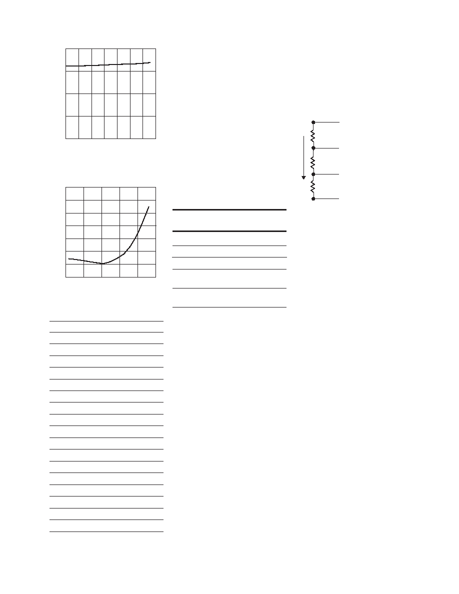
θch-b
Tch
(channel)
Tb (board
or belly
of the part)
Ta (ambient)
Ts (sink)
Pdiss
=
Vds
x
Ids
θb-s
θs-a
Figure 19. Equivalent Circuit for Thermal
Resistance.
Hence very similar to Ohms Law,
the temperature of the channel is
calculated with equation 8 below.
T
CH = P
diss (θch–b + θb– s + θs–a )
+ T
amb
(8)
If no heat sink is used or heat
sinking is incorporated into the
PCB board then equation 8 may
be reduced to:
T
CH = P
diss (θch–b + θb–a ) + Tamb (9)
where,
θ
b–a is the board to ambient
thermal resistance;
θ
ch–b is the channel to board
thermal resistance.
The board to ambient thermal
resistance thus becomes very
important for this is the
designer’s major source of heat
control. To demonstrate the
influence of
θ
b-a, thermal resis-
tance is measured for two very
different scenarios using the
ATF-521P8 demoboard. The first
case is done with just the
demoboard by itself. The second
case is the ATF demoboard
相關(guān)PDF資料 |
PDF描述 |
|---|---|
| ATF-521P8-BLK | C BAND, Si, N-CHANNEL, RF SMALL SIGNAL, HEMFET, MO-229 |
| ATF-521P8-TR2G | C BAND, Si, N-CHANNEL, RF SMALL SIGNAL, HEMFET, MO-229 |
| ATF-521P8-TR1G | C BAND, Si, N-CHANNEL, RF SMALL SIGNAL, HEMFET, MO-229 |
| ATF-521P8-BLKG | C BAND, Si, N-CHANNEL, RF SMALL SIGNAL, HEMFET, MO-229 |
| ATF-521P8-TR2 | L BAND, Si, N-CHANNEL, RF SMALL SIGNAL, HEMFET, MO-229 |
相關(guān)代理商/技術(shù)參數(shù) |
參數(shù)描述 |
|---|---|
| ATF524S16M | 制造商:n/a 功能描述:Inverter Semiconductor |
| ATF-53189 | 制造商:AGILENT 制造商全稱:AGILENT 功能描述:Enhancement Mode Pseudomorphic HEMT in SOT 89 Package |
| ATF-53189-BLK | 功能描述:射頻GaAs晶體管 Transistor GaAs High Linearity RoHS:否 制造商:TriQuint Semiconductor 技術(shù)類型:pHEMT 頻率:500 MHz to 3 GHz 增益:10 dB 噪聲系數(shù): 正向跨導(dǎo) gFS(最大值/最小值):4 S 漏源電壓 VDS: 閘/源擊穿電壓:- 8 V 漏極連續(xù)電流:3 A 最大工作溫度:+ 150 C 功率耗散:10 W 安裝風(fēng)格: 封裝 / 箱體: |
| ATF-53189-TR1 | 功能描述:射頻GaAs晶體管 Transistor GaAs High Linearity RoHS:否 制造商:TriQuint Semiconductor 技術(shù)類型:pHEMT 頻率:500 MHz to 3 GHz 增益:10 dB 噪聲系數(shù): 正向跨導(dǎo) gFS(最大值/最小值):4 S 漏源電壓 VDS: 閘/源擊穿電壓:- 8 V 漏極連續(xù)電流:3 A 最大工作溫度:+ 150 C 功率耗散:10 W 安裝風(fēng)格: 封裝 / 箱體: |
| ATF-53189-TR2 | 功能描述:射頻GaAs晶體管 Transistor GaAs Hi gh Linearity RoHS:否 制造商:TriQuint Semiconductor 技術(shù)類型:pHEMT 頻率:500 MHz to 3 GHz 增益:10 dB 噪聲系數(shù): 正向跨導(dǎo) gFS(最大值/最小值):4 S 漏源電壓 VDS: 閘/源擊穿電壓:- 8 V 漏極連續(xù)電流:3 A 最大工作溫度:+ 150 C 功率耗散:10 W 安裝風(fēng)格: 封裝 / 箱體: |
發(fā)布緊急采購,3分鐘左右您將得到回復(fù)。