- 您現(xiàn)在的位置:買賣IC網(wǎng) > PDF目錄381446 > AT29C040A-15PI (ATMEL CORP) 8-Bit Shift Registers With 3-State Output Registers 16-PDIP -55 to 125 PDF資料下載
參數(shù)資料
| 型號(hào): | AT29C040A-15PI |
| 廠商: | ATMEL CORP |
| 元件分類: | DRAM |
| 英文描述: | 8-Bit Shift Registers With 3-State Output Registers 16-PDIP -55 to 125 |
| 中文描述: | 512K X 8 FLASH 5V PROM, 150 ns, PDIP32 |
| 封裝: | 0.600 INCH, PLASTIC, DIP-32 |
| 文件頁數(shù): | 2/11頁 |
| 文件大小: | 234K |
| 代理商: | AT29C040A-15PI |
(continued)
To allow for simple in-system reprogrammability, the
AT29C040A does not require high input voltages for pro-
gramming. Five-volt-only commands determine the opera-
tion of the device. Reading data out of the device is similar
to reading from an EPROM. Reprogramming the
AT29C040A is performed on a sector basis; 256-bytes of
data are loaded into the device and then simultaneously
programmed.
Description
(Continued)
Device Operation
READ:
The AT29C040A is accessed like an EPROM.
When CE and OE are low and WE is high, the data stored
at the memory location determined by the address pins is
asserted on the outputs. The outputs are put in the high
impedance state whenever CE or OE is high. This dual-
line control gives designers flexibility in preventing bus
contention.
BYTE LOAD:
Byte loads are used to enter the 256-
bytes of a sector to be programmed or the software codes
for data protection. A byte load is performed by applying a
low pulse on the WE or CE input with CE or WE low (re-
spectively) and OE high. The address is latched on the
falling edge of CE or WE, whichever occurs last. The data
is latched by the first rising edge of CE or WE.
PROGRAM:
The device is reprogrammed on a sector
basis. If a byte of data within a sector is to be changed,
data for the entire sector must be loaded into the device.
Any byte that is not loaded during the programming of its
sector will be erased to read FFH. Once the bytes of a
sector are loaded into the device, they are simultaneously
programmed during the internal programming period. Af-
ter the first data byte has been loaded into the device, suc-
cessive bytes are entered in the same manner. Each new
byte to be programmed must have its high to low transition
on WE (or CE) within 150
μ
s of the low to high transition of
WE (or CE) of the preceding byte. If a high to low transition
is not detected within 150
μ
s of the last low to high transi-
tion, the load period will end and the internal programming
period will start. A8 to A18 specify the sector address. The
sector address must be valid during each high to low tran-
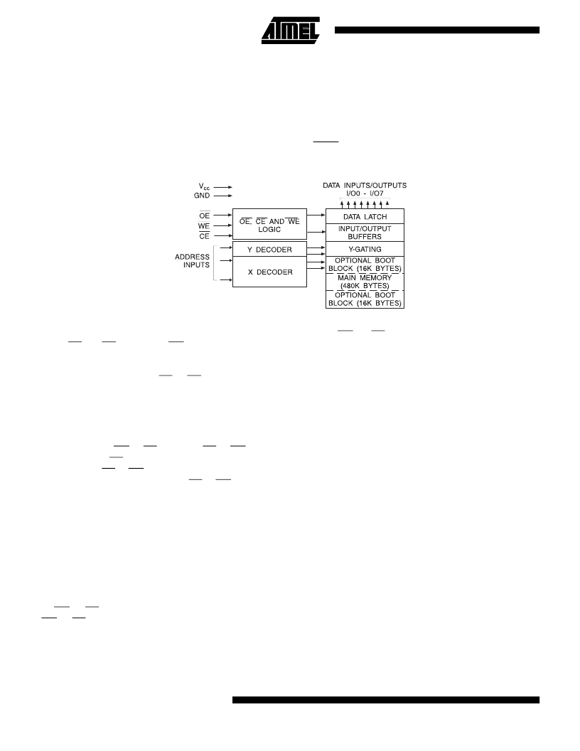
Block Diagram
During a reprogram cycle, the address locations and 256-
bytes of data are internally latched, freeing the address
and data bus for other operations. Following the initiation
of a program cycle, the device will automatically erase the
sector and then program the latched data using an internal
control timer. The end of a program cycle can be detected
by DATA polling of I/O7. Once the end of a program cycle
has been detected, a new access for a read or program
can begin.
sition of WE (or CE). A0 to A7 specify the byte address
within the sector. The bytes may be loaded in any order;
sequential loading is not required. Once a programming
operation has been initiated, and for the duration of t
WC
, a
read operation will effectively be a polling operation.
SOFTWARE DATA PROTECTION:
A software control-
led data protection feature is available on the AT29C040A.
Once the software protection is enabled a software algo-
rithm must be issued to the device before a program may
be performed. The software protection feature may be en-
abled or disabled by the user; when shipped from Atmel,
the software data protection feature is disabled. To enable
the software data protection, a series of three program
commands to specific addresses with specific data must
be performed. After the software data protection is en-
abled the same three program commands must begin
each program cycle in order for the programs to occur. All
software program commands must obey the sector pro-
gram timing specifications. The SDP feature protects all
sectors, not just a single sector. Once set, the software
data protection feature remains active unless its disable
command is issued. Power transitions will not reset the
software data protection feature, however the software
feature will guard against inadvertent program cycles dur-
ing power transitions.
After setting SDP, any attempt to write to the device with-
out the three-byte command sequence will start the inter-
nal write timers. No data will be written to the device; how-
ever, for the duration of t
WC
, a read operation will effec-
tively be a polling operation.
2
AT29C040A
相關(guān)PDF資料 |
PDF描述 |
|---|---|
| AT29C040A-15TC | 4-Megabit 512K x 8 5-volt Only 256-Byte Sector CMOS Flash Memory |
| AT29C040 | High Speed CMOS Logic Octal Positive-Edge-Triggered D-Type Flip-Flops with 3-State Outputs 20-PDIP -55 to 125 |
| AT29C040A-10 | High Speed CMOS Logic Octal Positive-Edge-Triggered D-Type Flip-Flops with 3-State Outputs 20-SOIC -55 to 125 |
| AT29C040A-10PC | High Speed CMOS Logic Octal Positive-Edge-Triggered D-Type Flip-Flops with 3-State Outputs 20-SOIC -55 to 125 |
| AT29C040A-10PI | High Speed CMOS Logic Octal Positive-Edge-Triggered D-Type Flip-Flops with 3-State Outputs 20-SOIC -55 to 125 |
相關(guān)代理商/技術(shù)參數(shù) |
參數(shù)描述 |
|---|---|
| AT29C040A-15TC | 功能描述:閃存 4M(512Kx8) 5V ONLY- 150NS COM TEMP RoHS:否 制造商:ON Semiconductor 數(shù)據(jù)總線寬度:1 bit 存儲(chǔ)類型:Flash 存儲(chǔ)容量:2 MB 結(jié)構(gòu):256 K x 8 定時(shí)類型: 接口類型:SPI 訪問時(shí)間: 電源電壓-最大:3.6 V 電源電壓-最小:2.3 V 最大工作電流:15 mA 工作溫度:- 40 C to + 85 C 安裝風(fēng)格:SMD/SMT 封裝 / 箱體: 封裝:Reel |
| AT29C040A-15TI | 功能描述:閃存 4M(512Kx8) 5V ONLY 150NS IND TEMP RoHS:否 制造商:ON Semiconductor 數(shù)據(jù)總線寬度:1 bit 存儲(chǔ)類型:Flash 存儲(chǔ)容量:2 MB 結(jié)構(gòu):256 K x 8 定時(shí)類型: 接口類型:SPI 訪問時(shí)間: 電源電壓-最大:3.6 V 電源電壓-最小:2.3 V 最大工作電流:15 mA 工作溫度:- 40 C to + 85 C 安裝風(fēng)格:SMD/SMT 封裝 / 箱體: 封裝:Reel |
| AT29C040A-20DC | 制造商:未知廠家 制造商全稱:未知廠家 功能描述:x8 Flash EEPROM |
| AT29C040A20DI | 制造商:ATMEL 功能描述:New |
| AT29C040A-20DI | 制造商:未知廠家 制造商全稱:未知廠家 功能描述:x8 Flash EEPROM |
發(fā)布緊急采購,3分鐘左右您將得到回復(fù)。