- 您現(xiàn)在的位置:買賣IC網(wǎng) > PDF目錄382860 > AS7C33256FT18B-75TQC (ALLIANCE SEMICONDUCTOR CORP) 3.3V 256K x 18 Flow Through Synchronous SRAM PDF資料下載
參數(shù)資料
| 型號(hào): | AS7C33256FT18B-75TQC |
| 廠商: | ALLIANCE SEMICONDUCTOR CORP |
| 元件分類: | DRAM |
| 英文描述: | 3.3V 256K x 18 Flow Through Synchronous SRAM |
| 中文描述: | 256K X 18 STANDARD SRAM, 7.5 ns, PQFP100 |
| 封裝: | 14 X 20 MM, TQFP-100 |
| 文件頁(yè)數(shù): | 4/19頁(yè) |
| 文件大小: | 401K |
| 代理商: | AS7C33256FT18B-75TQC |
第1頁(yè)第2頁(yè)第3頁(yè)當(dāng)前第4頁(yè)第5頁(yè)第6頁(yè)第7頁(yè)第8頁(yè)第9頁(yè)第10頁(yè)第11頁(yè)第12頁(yè)第13頁(yè)第14頁(yè)第15頁(yè)第16頁(yè)第17頁(yè)第18頁(yè)第19頁(yè)

AS7C33256FT18B
12/10/04; v.1.4
Alliance Semiconductor
P. 4 of 19
Functional description
The AS7C33256FT18B is a high-performance CMOS 4-Mbit synchronous Static Random Access Memory (SRAM) device organized as
262,144 words × 18 bits.
Fast cycle times of 7.5/8.5/10/12 ns with clock access times (t
CD
) of 6.5/7.5/8.0/10 ns. Three chip enable (CE) inputs permit easy memory
expansion. Burst operation is initiated in one of two ways: the controller address strobe (ADSC), or the processor address strobe (ADSP).
The burst advance pin (ADV) allows subsequent internally generated burst addresses.
Read cycles are initiated with ADSP (regardless of WE and ADSC) using the new external address clocked into the on-chip address register
when ADSP is sampled low, the chip enables are sampled active, and the output buffer is enabled with OE. In a read operation, the data
accessed by the current address registered in the address registers by the positive edge of CLK are carried to the data-out buffer. ADV is
ignored on the clock edge that samples ADSP asserted, but is sampled on all subsequent clock edges. Address is incremented internally for
the next access of the burst when ADV is sampled low and both address strobes are high. Burst mode is selectable with the
LBO
input. With
LBO
unconnected or driven high, burst operations use an interleaved count sequence. With
LBO
driven low, the device uses a linear count
sequence.
Write cycles are performed by disabling the output buffers with OE and asserting a write command. A global write enable GWE writes all 18
bits regardless of the state of individual BW[a,b] inputs. Alternately, when GWE is high, one or more bytes may be written by asserting
BWE and the appropriate individual byte BWn signals.
BWn is ignored on the clock edge that samples ADSP low, but it is sampled on all subsequent clock edges. Output buffers are disabled when
BWn is sampled LOW regardless of OE. Data is clocked into the data input register when BWn is sampled low. Address is incremented
internally to the next burst address if BWn and ADV are sampled low.
Read or write cycles may also be initiated with ADSC instead of ADSP. The differences between cycles initiated with ADSC and ADSP are
as follows:
ADSP must be sampled high when ADSC is sampled low to initiate a cycle with ADSC.
WE signals are sampled on the clock edge that samples ADSC low (and ADSP high).
Master chip enable CE0 blocks ADSP, but not ADSC.
The AS7C33256FT18B family operates from a core 3.3V power supply. I/Os use a separate power supply that can operate at 2.5V or 3.3V.
These devices are available in a 100-pin TQFP package.
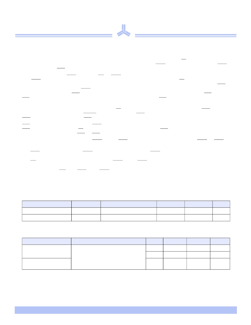
TQFP capacitance
*Guaranteed not tested
TQFP thermal resistance
Parameter
Symbol
C
IN*
C
I/O*
Test conditions
Min
Max
Unit
Input capacitance
V
IN
= 0V
V
OUT
= 0V
-
5
pF
I/O capacitance
-
7
pF
Description
Conditions
Symbol
Typical
Units
Thermal resistance
(junction to ambient)
1
1 This parameter is sampled
Test conditions follow standard test methods and
procedures for measuring thermal impedance,
per EIA/JESD51
1–layer
θ
JA
θ
JA
40
°
C/W
4–layer
22
°
C/W
Thermal resistance
(junction to top of case)
1
θ
JC
8
°
C/W
相關(guān)PDF資料 |
PDF描述 |
|---|---|
| AS7C33256FT18B-75TQCN | 3.3V 256K x 18 Flow Through Synchronous SRAM |
| AS7C33256FT18B-75TQI | 3.3V 256K x 18 Flow Through Synchronous SRAM |
| AS7C33256FT18B-75TQIN | 3.3V 256K x 18 Flow Through Synchronous SRAM |
| AS7C33256FT18B-80TQC | 3.3V 256K x 18 Flow Through Synchronous SRAM |
| AS7C33256FT18B-80TQCN | 3.3V 256K x 18 Flow Through Synchronous SRAM |
相關(guān)代理商/技術(shù)參數(shù) |
參數(shù)描述 |
|---|---|
| AS7C33256FT18B-75TQCN | 制造商:ALSC 制造商全稱:Alliance Semiconductor Corporation 功能描述:3.3V 256K x 18 Flow Through Synchronous SRAM |
| AS7C33256FT18B-75TQI | 制造商:ALSC 制造商全稱:Alliance Semiconductor Corporation 功能描述:3.3V 256K x 18 Flow Through Synchronous SRAM |
| AS7C33256FT18B-75TQIN | 制造商:ALSC 制造商全稱:Alliance Semiconductor Corporation 功能描述:3.3V 256K x 18 Flow Through Synchronous SRAM |
| AS7C33256FT18B-80TQC | 制造商:ALSC 制造商全稱:Alliance Semiconductor Corporation 功能描述:3.3V 256K x 18 Flow Through Synchronous SRAM |
| AS7C33256FT18B-80TQCN | 制造商:ALSC 制造商全稱:Alliance Semiconductor Corporation 功能描述:3.3V 256K x 18 Flow Through Synchronous SRAM |
發(fā)布緊急采購(gòu),3分鐘左右您將得到回復(fù)。