- 您現(xiàn)在的位置:買(mǎi)賣(mài)IC網(wǎng) > PDF目錄382858 > AS535SIP (Electronic Theatre Controls, Inc.) 2.5 V Precision Reference / Amplifier PDF資料下載
參數(shù)資料
| 型號(hào): | AS535SIP |
| 廠(chǎng)商: | Electronic Theatre Controls, Inc. |
| 英文描述: | 2.5 V Precision Reference / Amplifier |
| 中文描述: | 2.5 V精密參考/放大器 |
| 文件頁(yè)數(shù): | 3/3頁(yè) |
| 文件大?。?/td> | 27K |
| 代理商: | AS535SIP |
2.5V Precision Reference / Amplifier
A/AS535
ASTEC Semiconductor
27
Electrical Characteristics
Electrical characteristics are guaranteed over the full junction temperature range (0-105
°
C). Ambient temperature must be derated
based upon power dissipation and package thermal characteristics. Unless otherwise stated, test conditions are: V
OUT
= V
REF
, VCC=5V
and I
OUT
= 1 mA.
Parameter Symbol Test Condition Min Typ Max Min Typ Max Units
Supply Voltage VCC 4 15 4 15 V
Supply Current ICC 0.5 1 0. 5 1 mA
Reference Voltage V
REF
T
J
= 25
°
C 2.475 2.500 2.525 2.488 2.500 2.513 V
Line Regulation
V
OUT
VCC
=4 to 15 V -1 -10 -1 -10
mV
Load Regulation
V
OUT
I
OUT
= 1 to 100 mA 1 50 1 50
mV
Temperature Deviation
V
OUT
0 < T
J
< 105
°
C 3 10 3 8
mV
Reference Input Current I
REF
0.1 0.4 0.1 0.4
μ
A
Amplifier open loop gain Av
70 80 70 80
dB
Amplifier Unity gain frequency F
1
C
LOAD
< 1nF 1 2 1 2
MhZ
Output Saturation Voltage V
SAT
I
OUT
=100mA 0.4 0.4 V
Off State Leakage I
LEAK
V
REF
= 0 V, V
OUT
= 15 V 0.04 500 0.04 500 nA
*Temperature deviation is defined as the maximum deviation of the reference over the given temperature range and does not imply an
incremental deviation at any given temperature.
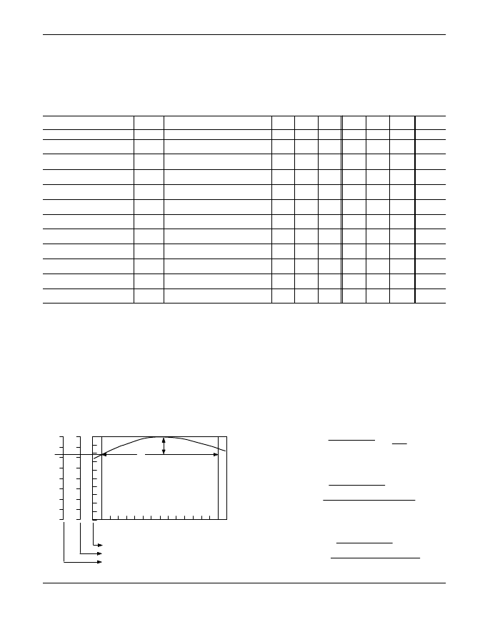
Typical Performance Curves
TC in mV/°C =
V
REF
T
A
TC in %/°C =
V
REF
V
REF
at 25° C
T
A
(
)
x 100
TC in ppm/°C =
V
REF
V
REF
at 25° C
T
A
(
)
x 10
6
*Calculating Average Temperature Coefficient (TC)
(mV)
Temperature (°C)
p
0
15
-10
0
30
45
60
75
90
105
%
0
m
-5
0.2
2000
0
V
REF
T
0.021 mV/°C
0.008 %/°C
8.0 ppm/°C
A535 (1.0 %)
AS535 (0.5 %)
相關(guān)PDF資料 |
PDF描述 |
|---|---|
| AS535D | 2.5 V Precision Reference / Amplifier |
| AS58C1001 | EEPROM |
| AS58C1001DCJ-20XT | EEPROM |
| AS58C1001DCJ-25883C | EEPROM |
| AS58C1001DCJ-25IT | EEPROM |
相關(guān)代理商/技術(shù)參數(shù) |
參數(shù)描述 |
|---|---|
| AS53600FLF | 制造商:TT Electronics / IRC 功能描述:AS53600FLF |
| AS53600HLF | 制造商:TT Electronics / IRC 功能描述:AS53600HLF |
| AS53600JLF | 制造商:TT Electronics / IRC 功能描述:AS53600JLF |
| AS53601FLF | 制造商:TT Electronics / IRC 功能描述:AS53601FLF |
| AS53601HLF | 制造商:TT Electronics / IRC 功能描述:AS53601HLF |
發(fā)布緊急采購(gòu),3分鐘左右您將得到回復(fù)。