- 您現(xiàn)在的位置:買賣IC網(wǎng) > PDF目錄362443 > AS4LC256K32S0-100TQC Synchronous Graphics RAM (SGRAM) PDF資料下載
參數(shù)資料
| 型號: | AS4LC256K32S0-100TQC |
| 英文描述: | Synchronous Graphics RAM (SGRAM) |
| 中文描述: | 同步圖形RAM(SGRAM) |
| 文件頁數(shù): | 8/15頁 |
| 文件大小: | 265K |
| 代理商: | AS4LC256K32S0-100TQC |
AS4LC4M4E0
AS4LC4M4E1
4/11/01; V1.1
Alliance Semiconductor
P. 8 of 15
Notes
1
2
3
I
CC1
, I
CC3
, I
CC4
, and I
CC6
are dependent on frequency.
I
CC1
and I
CC4
depend on output loading. Specified values are obtained with the output open.
An initial pause of 200 μs is required after power-up followed by any 8 RAS cycles before proper device operation is achieved. In the case of an internal
refresh counter, a minimum of 8 CAS-before-RAS initialization cycles instead of 8 RAS cycles are required. 8 initialization cycles are required after
extended periods of bias without clocks (greater than 8 ms).
AC Characteristics assume t
T
= 2 ns. All AC parameters are as described in AC test conditions below
V
IH
(min) and V
IL
(max) are reference levels for measuring timing of input signals. Transition times are measured between V
IH
and V
IL
.
Operation within the t
RCD
(max) limit insures that t
RAC
(max) can be met. t
RCD
(max) is specified as a reference point only. If t
RCD
is greater than the
specified t
RCD
(max) limit, then access time is controlled exclusively by t
CAC
.
Operation within the t
RAD
(max) limit insures that t
RAC
(max) can be met. t
RAD
(max) is specified as a reference point only. If t
RAD
is greater than the
specified t
RAD
(max) limit, then access time is controlled exclusively by t
AA
.
Assumes three state test load (5 pF and a 380
Thevenin equivalent).
Either t
RCH
or t
RRH
must be satisfied for a read cycle.
10 t
OFF
(max) defines the time at which the output achieves the open circuit condition; it is not referenced to output voltage levels. t
OFF
is referenced from
rising edge of RAS or CAS, whichever occurs last.
11 t
WCS
, t
WCH
, t
RWD
, t
CWD
and t
AWD
are not restrictive operating parameters. They are included in the datasheet as electrical characteristics only.
If t
WS
≥
t
WS
(min) and t
WH
≥
t
WH
(min), the cycle is an early write cycle and data out pins will remain open circuit, high impedance, throughout the
cycle. If t
RWD
≥
t
RWD
(min), t
CWD
≥
t
CWD
(min) and t
AWD
≥
t
AWD
(min), the cycle is a read-write cycle and the data out will contain data read from the
selected cell. If neither of the above conditions is satisfied, the condition of the data out at access time is indeterminate.
12 These parameters are referenced to CAS leading edge in early write cycles and to WE leading edge in read-write cycles.
13 Access time is determined by the longest of t
CAA
or t
CAC
or t
CPA
14 t
ASC
≥
t
CP
to achieve t
PC
(min) and t
CPA
(max) values.
15 These parameters are sampled and not 100% tested.
4
5
6
7
8
9
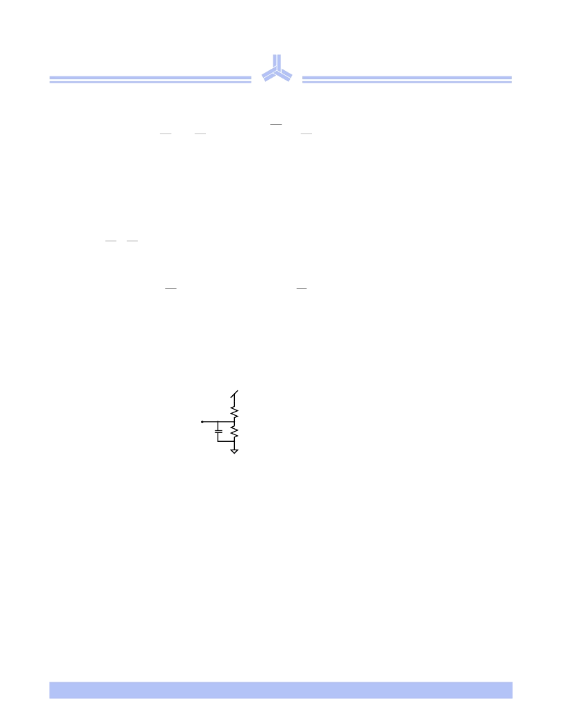
AC test conditions
- Access times are measured with output reference levels of V
OH
=
2.4V and V
OL
= 0.4V,
V
IH
= 2.0V and V
IL
= 0.8V
- Input rise and fall times: 2 ns
*including scope
and jig capacitance
50 pF*
R2 = 295
R1 = 828
D
out
GND
+3.3V
Figure B: Equivalent output load
(AS4LC4M4E0)
(AS4LC4M4E1)
相關(guān)PDF資料 |
PDF描述 |
|---|---|
| AS4LC256K32S0-133PQ | Synchronous Graphics RAM (SGRAM) |
| AS4LC256K32S0-133QC | Synchronous Graphics RAM (SGRAM) |
| AS4LC256K32S0-133TQC | Synchronous Graphics RAM (SGRAM) |
| AS4LC256K32S0-150PQ | Synchronous Graphics RAM (SGRAM) |
| AS4LC256K32S0-150QC | Synchronous Graphics RAM (SGRAM) |
相關(guān)代理商/技術(shù)參數(shù) |
參數(shù)描述 |
|---|---|
| AS4LC256K32S0-133PQ | 制造商:未知廠家 制造商全稱:未知廠家 功能描述:Synchronous Graphics RAM (SGRAM) |
| AS4LC256K32S0-133QC | 制造商:未知廠家 制造商全稱:未知廠家 功能描述:Synchronous Graphics RAM (SGRAM) |
| AS4LC256K32S0-133TQC | 制造商:未知廠家 制造商全稱:未知廠家 功能描述:Synchronous Graphics RAM (SGRAM) |
| AS4LC256K32S0-150PQ | 制造商:未知廠家 制造商全稱:未知廠家 功能描述:Synchronous Graphics RAM (SGRAM) |
| AS4LC256K32S0-150QC | 制造商:未知廠家 制造商全稱:未知廠家 功能描述:Synchronous Graphics RAM (SGRAM) |
發(fā)布緊急采購,3分鐘左右您將得到回復。