- 您現(xiàn)在的位置:買賣IC網(wǎng) > PDF目錄362423 > AS2845N (Electronic Theatre Controls, Inc.) Current Mode Controller PDF資料下載
參數(shù)資料
| 型號: | AS2845N |
| 廠商: | Electronic Theatre Controls, Inc. |
| 英文描述: | Current Mode Controller |
| 中文描述: | 電流模式控制器 |
| 文件頁數(shù): | 19/20頁 |
| 文件大小: | 94K |
| 代理商: | AS2845N |
ASTEC Semiconductor
Current Mode Controller
AS2842/3/4/5
55
graphically in Figure 22.
First, current-mode controllers detect and control
the peak inductor current, where as the
converter’s output corresponds to the average
inductor current. Figure 22(a) clearly shows that
the average inductor current (I
1
& I
2
) changes as
the duty ratio (D
1
& D
2
) changes. Note that for a
fixed control voltage, the peak current is the
same for any duty ratio. The difference between
the peak and average currents represents an
error which causes the converter to deviate from
true current-mode control.
Second, Figure 22(b) depicts how a small pertur-
bation of the inductor current (
I) can result in an
unstable condition. For duty ratios less than 50
%, the disturbance will quickly converge to a
steady state condition. For duty ratios greater
than 50 %,
I progressively increases on each
cycle, causing an unstable condition.
Both of these problems are corrected simulta-
neously by injecting a compensating ramp into
either the control voltage (V
E
) as shown in Figure
22(c) & (d), or to the current sense waveform at
pin 3. Since V
E
is not directly accessible, and, a
positive ramp waveform is readily available from
the oscillator at pin 4, it is more practical to add
the slope compensation to the current waveform.
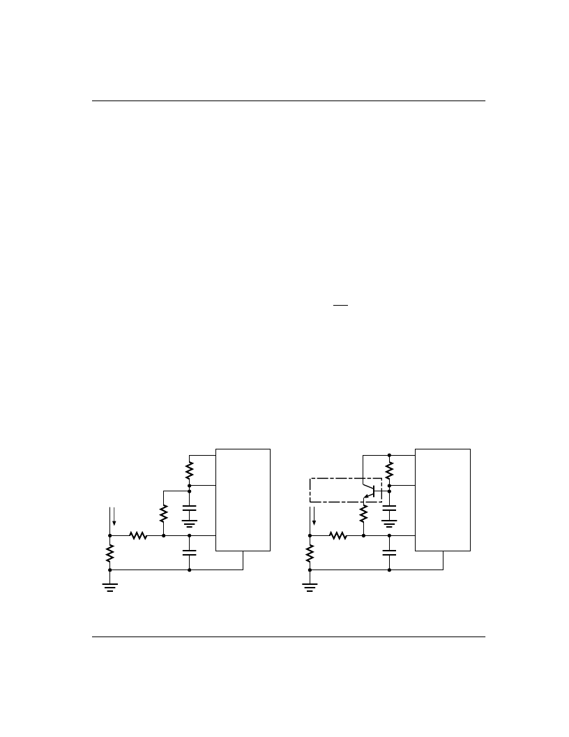
This can be implemented quite simply with the
addition of a single resistor, R
SLOPE
, between pin
4 and pin 3 as shown in Figure 23(a). R
SLOPE,
in
conjunction with the leading edge filter resistor,
R
1
(Section 2.1), forms a divider network which
determines the amount of slope added to the
waveform. The amount of slope added to the
current waveform is inversely proportional to the
value of R
SLOPE
. It has been determined that the
amount of slope (m) required is equal to or
greater than 1/2 the downslope (m
2
) of the induc-
tor current. Mathematically stated:
m
≥
m
2
2
(7)
In some cases the required value of R
SLOPE
may
be low enough to affect the oscillator circuit and
thus cause the frequency to shift. An emitter
follower circuit can be used as a buffer for R
SLOPE
as depicted in Figure 23(b).
Slope compensation can also be used to improve
noise immunity in current mode converters oper-
ating at less than 50% duty ratio. Power supplies
Figure 23.
Slope Compensation
R
SLOPE
R
1
I
SENSE
I
S
R
S
R
T
8
4
V
REG
R
T
/C
T
AS2842
3
5
GND
C
T
R
SLOPE
R
1
I
SENSE
I
S
R
S
R
T
8
4
V
REG
R
T
/C
T
AS2842
3
5
GND
C
T
(a)
(b)
OPTIONAL
BUFFER
相關(guān)PDF資料 |
PDF描述 |
|---|---|
| AS2850AT-1.5 | Analog IC |
| AS2850 | 5A Low Dropout Voltage Regulator Adjustable & Fixed Output, Fast Response |
| AS2850AT-2.5 | Analog IC |
| AS2850AT-3.3 | Analog IC |
| AS2850AT-5.0 | Analog IC |
相關(guān)代理商/技術(shù)參數(shù) |
參數(shù)描述 |
|---|---|
| AS284R5FLF | 制造商:TT Electronics / IRC 功能描述:AS284R5FLF |
| AS284R5HLF | 制造商:TT Electronics / IRC 功能描述:AS284R5HLF |
| AS284R5JLF | 制造商:TT Electronics / IRC 功能描述:AS284R5JLF |
| AS2850 | 制造商:SIPEX 制造商全稱:Sipex Corporation 功能描述:5A Low Dropout Voltage Regulator Adjustable & Fixed Output, Fast Response |
| AS2850AT | 制造商:Alpha & Omega Semiconductor 功能描述: |
發(fā)布緊急采購,3分鐘左右您將得到回復(fù)。