- 您現(xiàn)在的位置:買賣IC網(wǎng) > PDF目錄362423 > AS2840AU Analog IC PDF資料下載
參數(shù)資料
| 型號(hào): | AS2840AU |
| 英文描述: | Analog IC |
| 中文描述: | 模擬IC |
| 文件頁(yè)數(shù): | 14/20頁(yè) |
| 文件大?。?/td> | 94K |
| 代理商: | AS2840AU |
第1頁(yè)第2頁(yè)第3頁(yè)第4頁(yè)第5頁(yè)第6頁(yè)第7頁(yè)第8頁(yè)第9頁(yè)第10頁(yè)第11頁(yè)第12頁(yè)第13頁(yè)當(dāng)前第14頁(yè)第15頁(yè)第16頁(yè)第17頁(yè)第18頁(yè)第19頁(yè)第20頁(yè)
AS2842/3/4/5
Current Mode Controller
ASTEC Semiconductor
50
ing. Standard 2842 devices specify or trim only
for a specific value of discharge current. This
makes precise and repeatable duty ratio clamp-
ing virtually impossible due to other IC toler-
ances. The AS2844/5 provides true 50% duty
ratio clamping by virtue of excluding from its flip-
flop scheme, the normal output blanking associ-
ated with the discharge of C
T
. Standard AS2844/
5 devices include the output blanking associated
with the discharge of C
T
, resulting in somewhat
less than a 50% duty ratio.
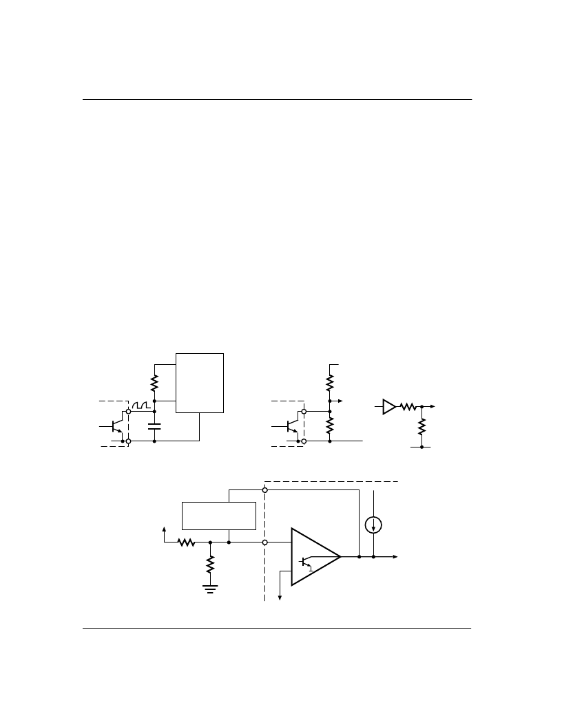
1.3.3 Synchronization
The advanced design of the AS2842 oscillator
simplifies synchronizing the frequency of two or
more devices to each other or to an external
clock. The R
T
/C
T
doubles as a synchronization
input which can easily be driven from any open
collector logic output. Figure 16 shows some
simple circuits for implementing synchroniza-
tion.
8
1.4 Error amplifier (COMP)
The AS2842 error amplifier is a wide bandwidth,
internally compensated operational amplifier
which provides a high DC open loop gain (90 dB).
The input to the amplifier is a PNP differential
pair. The non-inverting (+) input is internally
connected to the 2.5 V reference, and the invert-
ing (–) input is available at pin 2 (V
FB
). The output
of the error amplifier consists of an active pull-
down and a 0.8 mA current source pull-up as
shown in Figure 17. This type of output stage
allows easy implementation of soft start, latched
shutdown and reduced current sense clamp func-
tions. It also permits wire “OR-ing” of the error
amplifier outputs of several 2842s, or complete
bypass of the error amplifier when its output is
forced to remain in its “pull-up” condition.
Figure 16.
Synchronization
Figure 17.
Error Amplifier Compensation
+
–
COMPENSATION
NETWORK
2.50 V
TO
PWM
E/A
1 COMP
V
FB
2
0.8 mA
V
OUT
From
V
REG
A 2842
R
T
/C
T
GND
5
4
R
T
C
T
Open
Collector
Output
5 V
R
T
/C
T
Open
Collector
Output
3 K
2 K
2 K
R
T
/C
T
3 K
CMOS
SYNC
EXTERNAL CLOCK
相關(guān)PDF資料 |
PDF描述 |
|---|---|
| AS2842 | Current Mode Controller |
| AS2843 | Current Mode Controller |
| AS2844 | Current Mode Controller |
| AS2845D-8 | Current Mode Controller |
| AS2845N | Current Mode Controller |
相關(guān)代理商/技術(shù)參數(shù) |
參數(shù)描述 |
|---|---|
| AS2842 | 制造商:未知廠家 制造商全稱:未知廠家 功能描述:Current Mode Controller |
| AS2843 | 制造商:未知廠家 制造商全稱:未知廠家 功能描述:Current Mode Controller |
| AS2844 | 制造商:未知廠家 制造商全稱:未知廠家 功能描述:Current Mode Controller |
| AS2845 | 制造商:未知廠家 制造商全稱:未知廠家 功能描述:Current Mode Controller |
| AS28450FLF | 制造商:TT Electronics / IRC 功能描述:AS28450FLF |
發(fā)布緊急采購(gòu),3分鐘左右您將得到回復(fù)。