- 您現(xiàn)在的位置:買(mǎi)賣(mài)IC網(wǎng) > PDF目錄362332 > AN4504 IGBT ratings and characteristics PDF資料下載
參數(shù)資料
| 型號(hào): | AN4504 |
| 英文描述: | IGBT ratings and characteristics |
| 中文描述: | IGBT的收視率和特點(diǎn) |
| 文件頁(yè)數(shù): | 1/2頁(yè) |
| 文件大?。?/td> | 41K |
| 代理商: | AN4504 |
1/2
AN4502 Application Note
www.dynexsemi.com
AN4502
IGBT Electrostatic Handling Precautions
Application Note
AN4502-3.1 July 2002
Replaces September 2000 version, AN4502-3.0
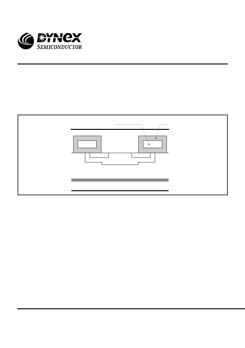
Fig. 1 Device silicon cross section
n+
n+
p+
n- base
n+ buffer layer
p+ substrate layer
Gate polysilicon
Oxide
Emitter contact
Collector contact
The IGBT has been developed to combine the properties of both
MOSFET and Bipolar devices. This overcomes some of the
limitations of both enabling high voltages to be switched and
high currents to be controlled with the use of relatively simple
gate drive circuitry. The active component, the silicon chip, has
a metal gate contact which is isolated from the underlying p-n
structure by a thin oxide layer (see fig 1.)
In order to achieve the required switching characteristics, this
structure requires a design in which the oxide layer is a few
hundred angstroms thick. For this reason manufacturers limit
the gate-emitter voltage to <
±
20V. If this voltage is exceeded
there is a danger that the chip will be destroyed and its control
action lost due to the gate-emitter structure becoming degraded.
As well as the possibility of such voltages occurring in the circuit
they can result from the accumulation of electrostatic charge.
Precautions must therefore be taken to avoid such damage.
IGBT products shipped from the Dynex Semiconductor factory
have a physical conducting material connecting the gate to
emitter and/or are packed in anti static conducting material. It is
important that the terminals are not touched by hand unless the
individual handling them is on an anti-static surface and /or is
grounded by an earthing wrist strap. Modules should only be
handled by their base. If it is necessary to touch the terminals
the individual should take the precaution of discharging
themselves to earth via a high value resistor (typically 2 to 4M
)
or preferably be earthed via a wrist strap. The conductive link
between the gate and emitter should be retained in place and
only removed immediately prior to wiring.
Care should be taken to ensure that any tools used, particularly
soldering irons, have a low resistance to earth. Note 1: For
further detail regarding the protection of electrostatic sensitive
devices the reader is recommended to consult British Standard
BS CECC 00015 entitled Basic Specification: Protection of
Electrostatic Sensitive Devices.
This documentation is available from:
BSI Customer Services,
BSI Standards,
389 Chiswick High Road,
London. W4 4AL.
United Kingdom.
Tel: + 44 (0) 208 996 7000
Fax: + 44 (0)208 996 7001
相關(guān)PDF資料 |
PDF描述 |
|---|---|
| AN4507 | Gate drive considerations to maximise IGBT efficiency |
| AN5011 | TV Channel Selector Circuit |
| AN5013K | TV Channel Selector Circuit |
| AN5015K | RF inductor, ceramic core, 2% tol, SMT, RoHS |
| AN501 | Circular Connector; No. of Contacts:19; Series:D38999; Body Material:Metal; Connecting Termination:Crimp; Connector Shell Size:15; Circular Contact Gender:Socket; Circular Shell Style:Straight Plug; Insert Arrangement:15-19 |
相關(guān)代理商/技術(shù)參數(shù) |
參數(shù)描述 |
|---|---|
| AN4505 | 制造商:DYNEX 制造商全稱(chēng):Dynex Semiconductor 功能描述:Power Assemblies |
| AN4506 | 制造商:DYNEX 制造商全稱(chēng):Dynex Semiconductor 功能描述:Power Assemblies |
| AN4507 | 制造商:未知廠家 制造商全稱(chēng):未知廠家 功能描述:Gate drive considerations to maximise IGBT efficiency |
| AN450C6AD4 | 制造商:AN# - MILITARY 功能描述: |
| AN450C8-6 | 制造商:AN# - MILITARY 功能描述: |
發(fā)布緊急采購(gòu),3分鐘左右您將得到回復(fù)。