- 您現(xiàn)在的位置:買(mǎi)賣(mài)IC網(wǎng) > PDF目錄382839 > AMS2502CS-3.0 (Advanced Monolithic Systems, Inc.) 1A VERY LOW DROPOUT VOLTAGE REGULATORS PDF資料下載
參數(shù)資料
| 型號(hào): | AMS2502CS-3.0 |
| 廠商: | Advanced Monolithic Systems, Inc. |
| 元件分類(lèi): | 基準(zhǔn)電壓源/電流源 |
| 英文描述: | 1A VERY LOW DROPOUT VOLTAGE REGULATORS |
| 中文描述: | 第1A非常低壓差電壓調(diào)節(jié)器 |
| 文件頁(yè)數(shù): | 6/8頁(yè) |
| 文件大小: | 75K |
| 代理商: | AMS2502CS-3.0 |

Advanced Monolithic Systems, Inc.
www.advanced-monolithic.com Phone (925) 443-0722 Fax (925) 443-0723
AMS2501/AMS2502
APPLICATION HINTS
Protection Diodes
Unlike older regulators, the AMS2501/AMS2502 family does not
need any protection diodes between the adjustment pin and the
output and from the output to the input to prevent die over-stress.
Internal resistors are limiting the internal current paths on the
AMS2501/AMS2502 adjustment pin, therefore even with bypass
capacitors on the adjust pin no protection diode is needed to
ensure device safety under short-circuit conditions. The Adjust pin
can be driven on a transient basis
±
7V with respect to the output
without any device degradation.
Diodes between the Output pin and V
POWER
pin are not usually
needed. Microsecond surge currents of 10A to 25A can be handled
by the internal diode between the Output pin and V
POWER
pin of
the device. In normal operations it is difficult to get those values
of surge currents even with the use of large output capacitances. If
high value output capacitors are used, such as 1000
μ
F to 5000
μ
F
and the V
POWER
pin is instantaneously shorted to ground, damage
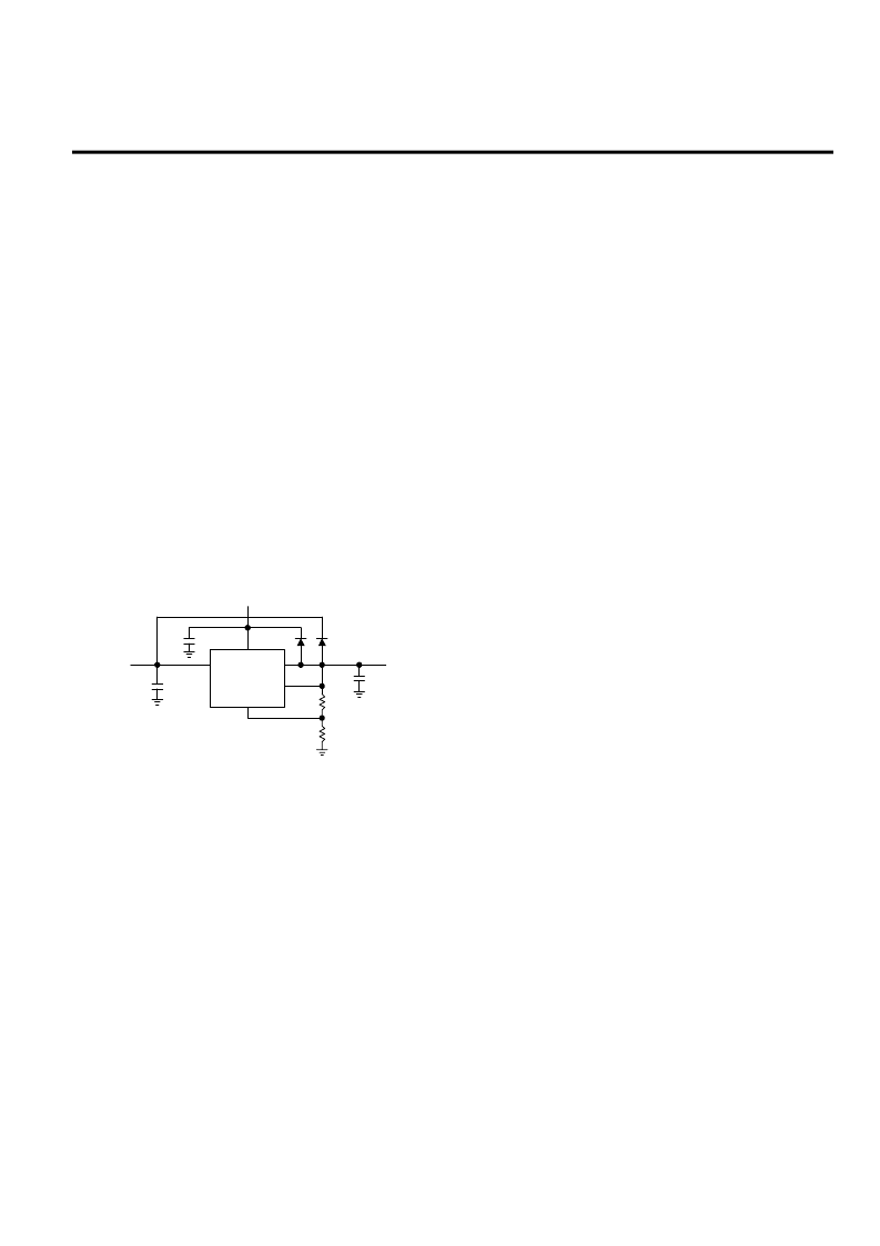
can occur. A diode from output to input is recommended, when a
crowbar circuit at the input of the AMS2501/AMS2502 is used
(Figure 6). Normal power supply cycling or even plugging and
unplugging in the system will not generate current large enough to
do any damage.
CONTROL
POWER OUTPUT
AMS2501
SENSE
ADJ
R1
R2
V
OUT
V
POWER
+
+
+
D2*
D1*
V
CONTROL
Figure 6. Optional Clamp Diodes Protect Against
Input Crowbar Circuits
If the AMS2501/AMS2502 is connected as a single supply device
with the control and power input pins shorted together the internal
diode between the output and the power input pin will protect the
control input pin. As with any IC regulator, none the protection
circuitry will be functional and the internal transistors will break
down if the maximum input to output voltage differential is
exceeded.
Thermal Considerations
The AMS2501/AMS2502 series have internal power and thermal
limiting circuitry designed to protect the device under overload
conditions. However maximum junction temperature ratings
should not be exceeded under continuous normal load conditions.
Careful consideration must be given to all sources of thermal
resistance from junction to ambient.
Control section can run up to 125
°
C, and the Power section can
run up to 150
°
C. Due to the thermal gradients between the power
transistor and the control circuitry there is a significant difference
in thermal resistance between the Control and Power sections.
Virtually all the power dissipated by the device is dissipated in the
power transistor. The temperature rise in the power transistor will
be greater than the temperature rise in the Control section making
the thermal resistance lower in the Control section. At power
levels below 0.5W the temperature gradient will be less than 25
°
C
and the maximum ambient temperature will be determined by the
junction temperature of the Control section. This is due to the
lower maximum junction temperature in the Control section. At
power levels above 0.5W the temperature gradient will be greater
than 25
°
C and the maximum ambient temperature will be
determined by the Power section. In both cases the junction
temperature is determined by the total power dissipated in the
device. For most low dropout applications the power dissipation
will be less than 0.5W.
The power in the device is made up of two components: the power
in the output transistor and the power in the drive circuit. The
power in the control circuit is negligible.
The power in the drive circuit is equal to:
P
DRIVE
= (V
CONTROL
- V
OUT
)(I
CONTROL
)
where I
CONTROL
is equal to between I
OUT
/100(typ) and
I
OUT
/60(max).
The power in the output transistor is equal to:
P
OUTPUT
= (V
POWER
-V
OUT
)(I
OUT
)
The total power is equal to:
P
TOTAL
= P
DRIVE
+ P
OUTPUT
Junction-to-case thermal resistance is specified from the IC
junction to the bottom of the case directly below the die. This is
the lowest resistance path for the heat flow. In order to ensure the
best possible thermal flow from this area of the package to the
PCB proper mounting is required.
相關(guān)PDF資料 |
PDF描述 |
|---|---|
| AMS2502CS-3.3 | 1A VERY LOW DROPOUT VOLTAGE REGULATORS |
| AMS2502CS-3.5 | 1A VERY LOW DROPOUT VOLTAGE REGULATORS |
| AMS2502CS-5.0 | 1A VERY LOW DROPOUT VOLTAGE REGULATORS |
| AMS2501CS-1.5 | 1A VERY LOW DROPOUT VOLTAGE REGULATORS |
| AMS2501CS-1.8 | 1A VERY LOW DROPOUT VOLTAGE REGULATORS |
相關(guān)代理商/技術(shù)參數(shù) |
參數(shù)描述 |
|---|---|
| AMS2502CS-33 | 制造商:ADMOS 制造商全稱(chēng):ADMOS 功能描述:1A VERY LOW DROPOUT VOLTAGE REGULATORS |
| AMS2502CS-35 | 制造商:ADMOS 制造商全稱(chēng):ADMOS 功能描述:1A VERY LOW DROPOUT VOLTAGE REGULATORS |
| AMS2502CS-5.0 | 制造商:ADMOS 制造商全稱(chēng):ADMOS 功能描述:1A VERY LOW DROPOUT VOLTAGE REGULATORS |
| AMS2502CS-50 | 制造商:ADMOS 制造商全稱(chēng):ADMOS 功能描述:1A VERY LOW DROPOUT VOLTAGE REGULATORS |
| AMS255 | 制造商:ADMOS 制造商全稱(chēng):ADMOS 功能描述:MICROPOWER SHUNT VOLTAGE REFERENCE |
發(fā)布緊急采購(gòu),3分鐘左右您將得到回復(fù)。