- 您現(xiàn)在的位置:買賣IC網(wǎng) > PDF目錄375310 > AM75PDL193CHHA70I (SPANSION LLC) 128 Megabit (8 M x 16-Bit) CMOS 3.0 Volt-only, Simultaneous Read/Write Flash Memory PDF資料下載
參數(shù)資料
| 型號(hào): | AM75PDL193CHHA70I |
| 廠商: | SPANSION LLC |
| 元件分類: | 存儲(chǔ)器 |
| 英文描述: | 128 Megabit (8 M x 16-Bit) CMOS 3.0 Volt-only, Simultaneous Read/Write Flash Memory |
| 中文描述: | SPECIALTY MEMORY CIRCUIT, PBGA73 |
| 封裝: | 9 X 13 MM, FBGA-73 |
| 文件頁(yè)數(shù): | 81/129頁(yè) |
| 文件大小: | 852K |
| 代理商: | AM75PDL193CHHA70I |
第1頁(yè)第2頁(yè)第3頁(yè)第4頁(yè)第5頁(yè)第6頁(yè)第7頁(yè)第8頁(yè)第9頁(yè)第10頁(yè)第11頁(yè)第12頁(yè)第13頁(yè)第14頁(yè)第15頁(yè)第16頁(yè)第17頁(yè)第18頁(yè)第19頁(yè)第20頁(yè)第21頁(yè)第22頁(yè)第23頁(yè)第24頁(yè)第25頁(yè)第26頁(yè)第27頁(yè)第28頁(yè)第29頁(yè)第30頁(yè)第31頁(yè)第32頁(yè)第33頁(yè)第34頁(yè)第35頁(yè)第36頁(yè)第37頁(yè)第38頁(yè)第39頁(yè)第40頁(yè)第41頁(yè)第42頁(yè)第43頁(yè)第44頁(yè)第45頁(yè)第46頁(yè)第47頁(yè)第48頁(yè)第49頁(yè)第50頁(yè)第51頁(yè)第52頁(yè)第53頁(yè)第54頁(yè)第55頁(yè)第56頁(yè)第57頁(yè)第58頁(yè)第59頁(yè)第60頁(yè)第61頁(yè)第62頁(yè)第63頁(yè)第64頁(yè)第65頁(yè)第66頁(yè)第67頁(yè)第68頁(yè)第69頁(yè)第70頁(yè)第71頁(yè)第72頁(yè)第73頁(yè)第74頁(yè)第75頁(yè)第76頁(yè)第77頁(yè)第78頁(yè)第79頁(yè)第80頁(yè)當(dāng)前第81頁(yè)第82頁(yè)第83頁(yè)第84頁(yè)第85頁(yè)第86頁(yè)第87頁(yè)第88頁(yè)第89頁(yè)第90頁(yè)第91頁(yè)第92頁(yè)第93頁(yè)第94頁(yè)第95頁(yè)第96頁(yè)第97頁(yè)第98頁(yè)第99頁(yè)第100頁(yè)第101頁(yè)第102頁(yè)第103頁(yè)第104頁(yè)第105頁(yè)第106頁(yè)第107頁(yè)第108頁(yè)第109頁(yè)第110頁(yè)第111頁(yè)第112頁(yè)第113頁(yè)第114頁(yè)第115頁(yè)第116頁(yè)第117頁(yè)第118頁(yè)第119頁(yè)第120頁(yè)第121頁(yè)第122頁(yè)第123頁(yè)第124頁(yè)第125頁(yè)第126頁(yè)第127頁(yè)第128頁(yè)第129頁(yè)
January 14, 2004
Am75PDL191CHHa/Am75PDL193CHHa
79
A D V A N C E I N F O R M A T I O N
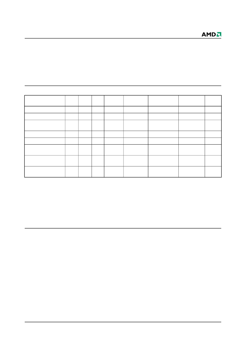
DEVICE BUS OPERATIONS
This section describes the requirements and use of
the device bus operations, which are initiated through
the internal command register. The command register
itself does not occupy any addressable memory loca-
tion. The register is a latch used to store the com-
mands, along with the address and data information
needed to execute the command. The contents of the
register serve as inputs to the internal state machine.
The state machine outputs dictate the function of the
device. Table 1 lists the device bus operations, the in-
puts and control levels they require, and the resulting
output. The following subsections describe each of
these operations in further detail.
Table 1.
Am29DL640H Device Bus Operations
Legend:
L = Logic Low = V
IL
, H = Logic High = V
IH
, V
ID
= 11.5–12.5 V, V
HH
= 9.0 ± 0.5 V, X = Don’t Care, SA = Sector Address,
A
IN
= Address In, D
IN
= Data In, D
OUT
= Data Out
Notes:
1. Addresses are A21:A0 in word mode.
2. The sector protect and sector unprotect functions may also be implemented via programming equipment. See the “Sector/Sector
Block Protection and Unprotection” section.
3. If WP#/ACC = V
IL
, sectors 0, 1, 140, and 141 remain protected. If WP#/ACC = V
IH
, protection on sectors 0, 1, 140, and 141
depends on whether they were last protected or unprotected using the method described in “Sector/Sector Block Protection
and Unprotection”. If WP#/ACC = V
HH
, all sectors will be unprotected.
Word/Byte Configuration
The BYTE# pin controls whether the device data I/O
pins operate in the byte or word configuration. If the
BYTE# pin is set at logic ‘1’, the device is in word con-
figuration, DQ15–DQ0 are active and controlled by
CE# and OE#.
If the BYTE# pin is set at logic ‘0’, the device is in byte
configuration, and only data I/O pins DQ7–DQ0 are
active and controlled by CE# and OE#. The data I/O
pins DQ14–DQ8 are tri-stated, and the DQ15 pin is
used as an input for the LSB (A-1) address function.
Requirements for Reading Array Data
To read array data from the outputs, the system must
drive the CE# and OE# pins to V
IL
. CE# is the power
control and selects the device. OE# is the output con-
trol and gates array data to the output pins. WE#
should remain at V
IH
. The BYTE# pin determines
whether the device outputs array data in words or
bytes.
The internal state machine is set for reading array data
upon device power-up, or after a hardware reset. This
ensures that no spurious alteration of the memory
content occurs during the power transition. No com-
mand is necessary in this mode to obtain array data.
Standard microprocessor read cycles that assert valid
addresses on the device address inputs produce valid
data on the device data outputs. Each bank remains
enabled for read access until the command register
contents are altered.
Operation
CE#
OE#
WE#
RESET#
WP#/ACC
Addresses
(Note 2)
DQ15–DQ8
DQ7–
DQ0
Read
L
L
H
H
L/H
A
IN
D
OUT
D
OUT
Write
L
H
L
H
(Note 3)
A
IN
D
IN
D
IN
Standby
V
CC
±
0.3 V
X
X
V
CC
±
0.3 V
L/H
X
High-Z
High-Z
Output Disable
L
H
H
H
L/H
X
High-Z
High-Z
Reset
X
X
X
L
L/H
X
High-Z
High-Z
Sector Protect (Note 2)
L
H
L
V
ID
L/H
SA, A6 = L,
A1 = H, A0 = L
X
D
IN
Sector Unprotect (Note 2)
L
H
L
V
ID
(Note 3)
SA, A6 = H,
A1 = H, A0 = L
X
D
IN
Temporary Sector
Unprotect
X
X
X
V
ID
(Note 3)
A
IN
D
IN
D
IN
相關(guān)PDF資料 |
PDF描述 |
|---|---|
| Am75PDL191CHH | 128 Megabit (8 M x 16-Bit) CMOS 3.0 Volt-only, Simultaneous Read/Write Flash Memory |
| AM75PDL191CHH_0402 | 128 Megabit (8 M x 16-Bit) CMOS 3.0 Volt-only, Simultaneous Read/Write Flash Memory |
| AM75PDL191CHH70I | 128 Megabit (8 M x 16-Bit) CMOS 3.0 Volt-only, Simultaneous Read/Write Flash Memory |
| Am75PDL193CHH | 128 Megabit (8 M x 16-Bit) CMOS 3.0 Volt-only, Simultaneous Read/Write Flash Memory |
| AM75PDL193CHH70I | 128 Megabit (8 M x 16-Bit) CMOS 3.0 Volt-only, Simultaneous Read/Write Flash Memory |
相關(guān)代理商/技術(shù)參數(shù) |
參數(shù)描述 |
|---|---|
| AM7630N | 制造商:ANALOGPOWER 制造商全稱:ANALOGPOWER 功能描述:N-Channel 30-V (D-S) MOSFET |
| AM7640N | 制造商:ANALOGPOWER 制造商全稱:ANALOGPOWER 功能描述:Dual N-Channel 40-V (D-S) MOSFET |
| AM7901ADC | 制造商:Advanced Micro Devices 功能描述:PCM CODEC, Single, 28 Pin, Ceramic, DIP |
| AM7901AJC | 制造商:未知廠家 制造商全稱:未知廠家 功能描述:u-Law/Linear CODEC |
| AM7901APC | 制造商:未知廠家 制造商全稱:未知廠家 功能描述:u-Law/Linear CODEC |
發(fā)布緊急采購(gòu),3分鐘左右您將得到回復(fù)。