- 您現(xiàn)在的位置:買賣IC網(wǎng) > PDF目錄366544 > Am53CF94JCW (Advanced Micro Devices, Inc.) Enhanced SCSI-2 Controller (ESC) PDF資料下載
參數(shù)資料
| 型號: | Am53CF94JCW |
| 廠商: | Advanced Micro Devices, Inc. |
| 英文描述: | Enhanced SCSI-2 Controller (ESC) |
| 中文描述: | 增強型SCSI - 2控制器(調(diào)速器) |
| 文件頁數(shù): | 16/76頁 |
| 文件大小: | 735K |
| 代理商: | AM53CF94JCW |
第1頁第2頁第3頁第4頁第5頁第6頁第7頁第8頁第9頁第10頁第11頁第12頁第13頁第14頁第15頁當前第16頁第17頁第18頁第19頁第20頁第21頁第22頁第23頁第24頁第25頁第26頁第27頁第28頁第29頁第30頁第31頁第32頁第33頁第34頁第35頁第36頁第37頁第38頁第39頁第40頁第41頁第42頁第43頁第44頁第45頁第46頁第47頁第48頁第49頁第50頁第51頁第52頁第53頁第54頁第55頁第56頁第57頁第58頁第59頁第60頁第61頁第62頁第63頁第64頁第65頁第66頁第67頁第68頁第69頁第70頁第71頁第72頁第73頁第74頁第75頁第76頁

P R E L I M I N A R Y
AMD
16
Am53CF94/Am53CF96
RSTC
Reset Control
(Output, Active Low, Open Drain)
This is a SCSI output with 48 mA drive. The Reset SCSI
command will cause the device to drive
RSTC
active for
25 ms–40 ms, which will depend on the CLK frequency
and the conversion factor. When the device is config-
ured in the Single Ended SCSI Mode (
DFMODE
inac-
tive) this pin is defined as a
RST
output for the SCSI bus.
When the device is configured in the Differential SCSI
Mode (
DFMODE
active) this pin is defined as the direc-
tion control for the external differential transceiver. In
this mode, a signal high state corresponds to an output
to the SCSI bus and a low state corresponds to an input
from the SCSI bus.
REQC
Request Control
(Output, Active Low, Open Drain)
This is a SCSI output with 48 mA drive. This signal is
activated only in the Target mode.
ACKC
Acknowledge Control
(Output, Active Low, Open Drain)
This is a SCSI output with 48 mA drive. This signal is ac-
tivated only in the Initiator mode.
ISEL
Initiator Select
(Output, Active High)
This signal is available on the Am53CF96 only. This sig-
nal is active whenever the device is in the Initiator mode.
In the differential mode this signal is used to enable the
Initiator signals
ACKC
and
ATN
and the device also
drives these signals.
TSEL
Target Select
(Output, Active High)
This signal is available on the Am53CF96 only. This sig-
nal is active whenever the device is in the Target mode.
In the differential mode this signal is used to enable the
Target signals
REQC
,
MSG
,
C/D
and
I/O
and the device
also drives these signals.
FUNCTIONAL DESCRIPTION
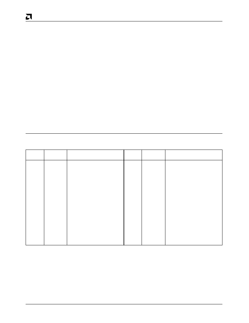
Register Map
Address
(Hex.) Operation
Register
00
Read
Current Transfer Count
Register Low
Start Transfer Count Register
Low
Current Transfer Count
Register Middle
Start Transfer Count Register
Middle
FIFO Register
Command Register
Status Register
SCSI Destination ID Register
Interrupt Status Register
SCSI Timeout Register
Internal State Register
Synchronous Transfer Period
Register
00
Write
01
Read
01
Write
02
03
04
04
05
05
06
06
Read/Write
Read/Write
Read
Write
Read
Write
Read
Write
Address
(Hex.)
Operation
Register
07
Read
Current FIFO/Internal State
Register
Synchronous Offset Register
Control Register 1
Clock Factor Register
Forced Test Mode Register
Control Register 2
Control Register 3
Control Register 4
Current Transfer Count
Register High
Start Transfer Count
Register High
Data Alignment Register
07
08
09
0A
0B
0C
0D
0E
Write
Read/Write
Write
Write
Read/Write
Read/Write
Read/Write
Read
0E
Write
0F
Write
Note:
Not all registers in this device are both readable and writable. Some read only registers share the same address with write only
registers. The registers can be accessed by asserting the
CS
signal and then asserting either
RD
or
WR
signal depending on the
operation to be performed. Only the FIFO Register can be accessed by asserting either
CS
or
DACK
n conjunction with
RD
and
WR
signals or
DMARD
and
DMAWR
signals. The register address inputs are ignored when
DACK
is used but must be valid
when
CS
is used.
相關(guān)PDF資料 |
PDF描述 |
|---|---|
| Am53CF94KC | Enhanced SCSI-2 Controller (ESC) |
| Am53CF94KCW | Enhanced SCSI-2 Controller (ESC) |
| Am53CF96 | Enhanced SCSI-2 Controller (ESC) |
| Am53CF96JC | Enhanced SCSI-2 Controller (ESC) |
| Am53CF96JCW | Enhanced SCSI-2 Controller (ESC) |
相關(guān)代理商/技術(shù)參數(shù) |
參數(shù)描述 |
|---|---|
| AM53CF94KC | 制造商:AMD 制造商全稱:Advanced Micro Devices 功能描述:Enhanced SCSI-2 Controller (ESC) |
| AM53CF94KCW | 制造商:AMD 制造商全稱:Advanced Micro Devices 功能描述:Enhanced SCSI-2 Controller (ESC) |
| AM53CF96 | 制造商:AMD 制造商全稱:Advanced Micro Devices 功能描述:Enhanced SCSI-2 Controller (ESC) |
| AM53CF96JC | 制造商:AMD 制造商全稱:Advanced Micro Devices 功能描述:Enhanced SCSI-2 Controller (ESC) |
| AM53CF96JCW | 制造商:AMD 制造商全稱:Advanced Micro Devices 功能描述:Enhanced SCSI-2 Controller (ESC) |
發(fā)布緊急采購,3分鐘左右您將得到回復(fù)。