- 您現(xiàn)在的位置:買賣IC網(wǎng) > PDF目錄366487 > AM29LV160DB-90SC (Advanced Micro Devices, Inc.) 16 Megabit (2 M x 8-Bit/1 M x 16-Bit) CMOS 3.0 Volt-only Boot Sector Flash Memory PDF資料下載
參數(shù)資料
| 型號: | AM29LV160DB-90SC |
| 廠商: | Advanced Micro Devices, Inc. |
| 元件分類: | FLASH |
| 英文描述: | 16 Megabit (2 M x 8-Bit/1 M x 16-Bit) CMOS 3.0 Volt-only Boot Sector Flash Memory |
| 中文描述: | 16Mb(2M×8位/1Mx16位), 3V, CMOS引導(dǎo)扇區(qū)閃存 |
| 文件頁數(shù): | 35/52頁 |
| 文件大?。?/td> | 844K |
| 代理商: | AM29LV160DB-90SC |
第1頁第2頁第3頁第4頁第5頁第6頁第7頁第8頁第9頁第10頁第11頁第12頁第13頁第14頁第15頁第16頁第17頁第18頁第19頁第20頁第21頁第22頁第23頁第24頁第25頁第26頁第27頁第28頁第29頁第30頁第31頁第32頁第33頁第34頁當前第35頁第36頁第37頁第38頁第39頁第40頁第41頁第42頁第43頁第44頁第45頁第46頁第47頁第48頁第49頁第50頁第51頁第52頁
22358B7
May 5, 2006
Am29LV160D
33
D A T A S H E E T
TEST CONDITIONS
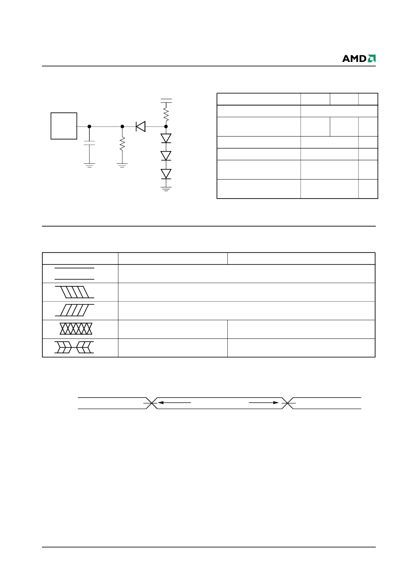
Table 11. Test Specifications
Key to Switching Waveforms
2.7 k
Ω
C
L
6.2 k
Ω
3.3 V
Device
Under
Test
Figure 11. Test Setup
Note:
Diodes are IN3064 or equivalent
Test Condition
-70
-90, -120
Unit
Output Load
1 TTL gate
Output Load Capacitance, C
L
(including jig capacitance)
30
100
pF
Input Rise and Fall Times
5
ns
Input Pulse Levels
0.0–3.0
V
Input timing measurement
reference levels
1.5
V
Output timing measurement
reference levels
1.5
V
WAVEFORM
INPUTS
OUTPUTS
Steady
Changing from H to L
Changing from L to H
Don’t Care, Any Change Permitted
Changing, State Unknown
Does Not Apply
Center Line is High Impedance State (High Z)
3.0 V
0.0 V
1.5 V
1.5 V
Output
Measurement Level
Input
Figure 12. Input Waveforms and Measurement Levels
相關(guān)PDF資料 |
PDF描述 |
|---|---|
| AM29LV160DB-90SD | 16 Megabit (2 M x 8-Bit/1 M x 16-Bit) CMOS 3.0 Volt-only Boot Sector Flash Memory |
| AM29LV160DB-90SF | 16 Megabit (2 M x 8-Bit/1 M x 16-Bit) CMOS 3.0 Volt-only Boot Sector Flash Memory |
| AM29LV160DB-70SE | 16 Megabit (2 M x 8-Bit/1 M x 16-Bit) CMOS 3.0 Volt-only Boot Sector Flash Memory |
| AM29LV160DB-70SI | 16 Megabit (2 M x 8-Bit/1 M x 16-Bit) CMOS 3.0 Volt-only Boot Sector Flash Memory |
| AM29LV160DB-70WCE | 16 Megabit (2 M x 8-Bit/1 M x 16-Bit) CMOS 3.0 Volt-only Boot Sector Flash Memory |
相關(guān)代理商/技術(shù)參數(shù) |
參數(shù)描述 |
|---|---|
| AM29LV160DT120EC | 制造商:AMD 功能描述:* |
| AM29LV160DT-70EC | 制造商:Advanced Micro Devices 功能描述: |
| AM29LV160DT-70EI | 制造商:Advanced Micro Devices 功能描述: |
| AM29LV160DT90EC | 制造商:Spansion 功能描述:Flash Mem Parallel 3V/3.3V 16M-Bit 2M x 8/1M x 16 90ns 48-Pin TSOP |
| AM29LV160DT-90EC | 制造商:Advanced Micro Devices 功能描述: 制造商:Advanced Micro Devices 功能描述:NOR Flash, 1M x 16, 48 Pin, Plastic, TSSOP 制造商:Analog Devices 功能描述:NOR Flash, 1M x 16, 48 Pin, Plastic, TSSOP |
發(fā)布緊急采購,3分鐘左右您將得到回復(fù)。