- 您現(xiàn)在的位置:買賣IC網 > PDF目錄362246 > AM29F100AT-70SE 30V Single N-Channel HEXFET Power MOSFET in a SOT-223 package; Similar to IRLL3303 with Lead Free Packaging PDF資料下載
參數資料
| 型號: | AM29F100AT-70SE |
| 英文描述: | 30V Single N-Channel HEXFET Power MOSFET in a SOT-223 package; Similar to IRLL3303 with Lead Free Packaging |
| 中文描述: | x8/x16閃存EEPROM |
| 文件頁數: | 13/39頁 |
| 文件大?。?/td> | 728K |
| 代理商: | AM29F100AT-70SE |
第1頁第2頁第3頁第4頁第5頁第6頁第7頁第8頁第9頁第10頁第11頁第12頁當前第13頁第14頁第15頁第16頁第17頁第18頁第19頁第20頁第21頁第22頁第23頁第24頁第25頁第26頁第27頁第28頁第29頁第30頁第31頁第32頁第33頁第34頁第35頁第36頁第37頁第38頁第39頁
Am29F002B/Am29F002NB
13
DQ7 or DQ6. See “Write Operation Status” for informa-
tion on these status bits.
Any commands written to the device during the
Embedded Program Algorithm are ignored. On the
Am29F002B only, note that a
hardware reset
during
the sector erase operation immediately terminates the
operation. The Sector Erase command sequence
should be reinitiated once the device has returned to
reading array data, to ensure data integrity.
Programming is allowed in any sequence and across
sector boundaries.
A bit cannot be programmed
from a “0” back to a “1”.
Attempting to do so may halt
the operation and set DQ5 to “1”, or cause the Data#
Polling algorithm to indicate the operation was suc-
cessful. However, a succeeding read will show that the
data is still “0”. Only erase operations can convert a “0”
to a “1”.
Note:
See the appropriate Command Definitions table for
program command sequence.
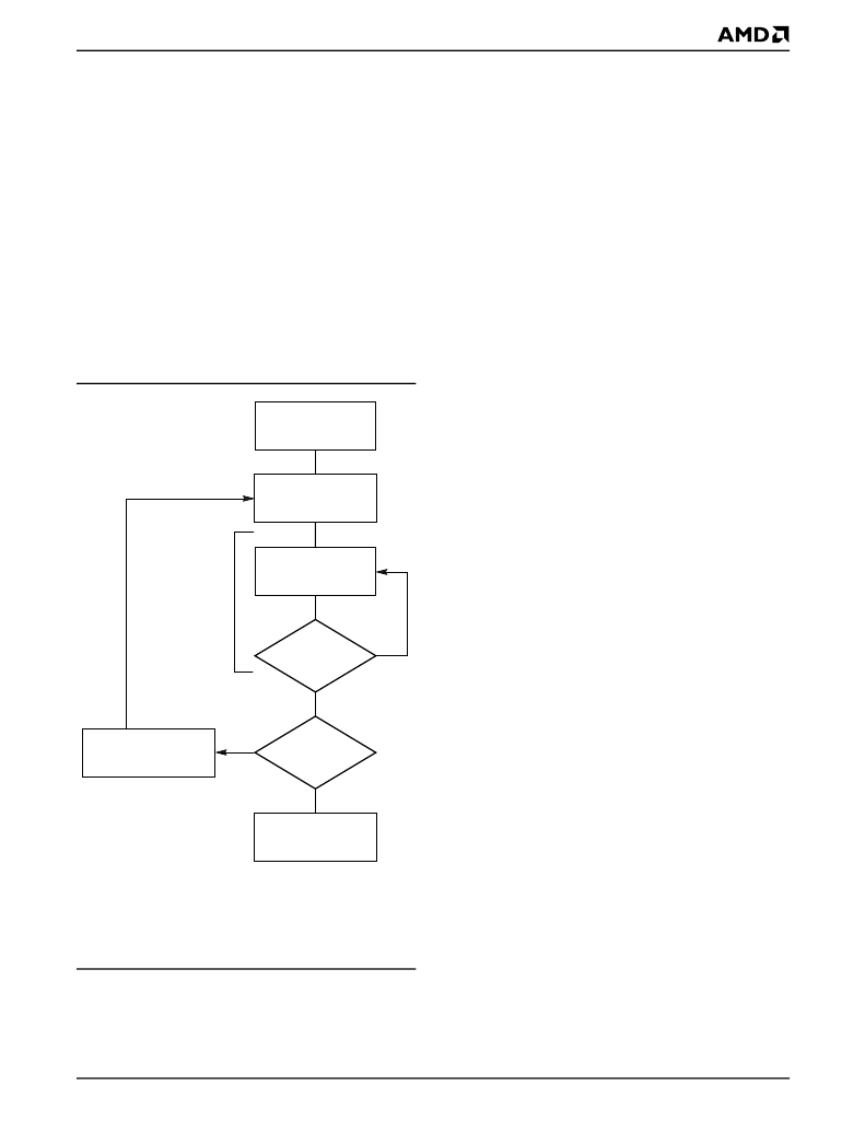
Figure 2.
Program Operation
Chip Erase Command Sequence
Chip erase is a six-bus-cycle operation. The chip erase
command sequence is initiated by writing two unlock
cycles, followed by a set-up command. Two additional
unlock write cycles are then followed by the chip erase
command, which in turn invokes the Embedded Erase
algorithm. The device does
not
require the system to
preprogram prior to erase. The Embedded Erase algo-
rithm automatically preprograms and verifies the entire
memory for an all zero data pattern prior to electrical
erase. The system is not required to provide any con-
trols or timings during these operations. The Command
Definitions table shows the address and data require-
ments for the chip erase command sequence.
Any commands written to the chip during the
Embedded Erase algorithm are ignored. On the
Am29F002B only, note that a
hardware reset
during
the sector erase operation immediately terminates the
operation. The Sector Erase command sequence
should be reinitiated once the device has returned to
reading array data, to ensure data integrity.
The system can determine the status of the erase oper-
ation by using DQ7, DQ6, or DQ2. See “Write
Operation Status” for information on these status bits.
When the Embedded Erase algorithm is complete, the
device returns to reading array data and addresses are
no longer latched.
Figure 3 illustrates the algorithm for the erase opera-
tion. See the Erase/Program Operations tables in “AC
Characteristics” for parameters, and to the Chip/Sector
Erase Operation Timings for timing waveforms.
Sector Erase Command Sequence
Sector erase is a six bus cycle operation. The sector
erase command sequence is initiated by writing two
unlock cycles, followed by a set-up command. Two
additional unlock write cycles are then followed by the
address of the sector to be erased, and the sector
erase command. The Command Definitions table
shows the address and data requirements for the
sector erase command sequence.
The device does
not
require the system to preprogram
the memory prior to erase. The Embedded Erase algo-
rithm automatically programs and verifies the sector for
an all zero data pattern prior to electrical erase. The
system is not required to provide any controls or
timings during these operations.
After the command sequence is written, a sector erase
time-out of 50 μs begins. During the time-out period,
additional sector addresses and sector erase com-
mands may be written. Loading the sector erase buffer
may be done in any sequence, and the number of
sectors may be from one sector to all sectors. The time
between these additional cycles must be less than 50
μs, otherwise the last address and command might not
be accepted, and erasure may begin. It is recom-
mended that processor interrupts be disabled during
this time to ensure all commands are accepted. The
START
Write Program
Command Sequence
Data Poll
from System
Verify Data
No
Yes
Last Address
No
Yes
Programming
Completed
Increment Address
Embedded
Program
algorithm
in progress
相關PDF資料 |
PDF描述 |
|---|---|
| AM29F100AT-70SI | x8/x16 Flash EEPROM |
| AM29F100AT-90EC | 20V Single N-Channel HEXFET Power MOSFET in a TO-220AB package; A IRL3102 with Standard Packaging |
| AM29F100AT-90EE | x8/x16 Flash EEPROM |
| AM29F100AT-90EI | 100V Single N-Channel HEXFET Power MOSFET in a TO-220AB package; A IRL530N with Standard Packaging |
| AM29F100AT-90FC | 55V Single N-Channel HEXFET Power MOSFET in a TO-262 package; A IRFZ24NL with Standard Packaging |
相關代理商/技術參數 |
參數描述 |
|---|---|
| AM29F100B120EC | 制造商:AMD 功能描述:* |
| AM29F100B-120EC | 制造商:Advanced Micro Devices 功能描述: |
| AM29F100B120SC | 制造商:AMD 功能描述:New |
| AM29F100B-120SC | 制造商:Advanced Micro Devices 功能描述:NOR Flash, 64K x 16, 44 Pin, Plastic, SOP |
| AM29F100B90SIT | 制造商:AMD 功能描述:New |
發(fā)布緊急采購,3分鐘左右您將得到回復。