- 您現(xiàn)在的位置:買賣IC網(wǎng) > PDF目錄375288 > AM29BDS128HE9VKI (SPANSION LLC) 128 or 64 Megabit (8 M or 4 M x 16-Bit) CMOS 1.8 Volt-only Simultaneous Read/Write, Burst Mode Flash Memory PDF資料下載
參數(shù)資料
| 型號: | AM29BDS128HE9VKI |
| 廠商: | SPANSION LLC |
| 元件分類: | DRAM |
| 英文描述: | 128 or 64 Megabit (8 M or 4 M x 16-Bit) CMOS 1.8 Volt-only Simultaneous Read/Write, Burst Mode Flash Memory |
| 中文描述: | 8M X 16 FLASH 1.8V PROM, 50 ns, PBGA80 |
| 封裝: | 11.50 X 9 MM, 0.80 MM PITCH, FPBGA-80 |
| 文件頁數(shù): | 14/89頁 |
| 文件大?。?/td> | 913K |
| 代理商: | AM29BDS128HE9VKI |
第1頁第2頁第3頁第4頁第5頁第6頁第7頁第8頁第9頁第10頁第11頁第12頁第13頁當前第14頁第15頁第16頁第17頁第18頁第19頁第20頁第21頁第22頁第23頁第24頁第25頁第26頁第27頁第28頁第29頁第30頁第31頁第32頁第33頁第34頁第35頁第36頁第37頁第38頁第39頁第40頁第41頁第42頁第43頁第44頁第45頁第46頁第47頁第48頁第49頁第50頁第51頁第52頁第53頁第54頁第55頁第56頁第57頁第58頁第59頁第60頁第61頁第62頁第63頁第64頁第65頁第66頁第67頁第68頁第69頁第70頁第71頁第72頁第73頁第74頁第75頁第76頁第77頁第78頁第79頁第80頁第81頁第82頁第83頁第84頁第85頁第86頁第87頁第88頁第89頁
12
Am29BDS128H/Am29BDS640H
27024B3 May 10, 2006
D A T A S H E E T
active clock edge, and how the RDY signal will transi-
tion with valid data. The system would then write the
configuration register command sequence. See
“Set
Configuration Register Command Sequence” section
on page 33
and
“Command Definitions” section on
page 33
for further details.
Once the system has written the “Set Configuration
Register” command sequence, the device is enabled
for synchronous reads only.
The initial word is output t
IACC
after the active edge of
the first CLK cycle. Subsequent words are output t
BACC
after the active edge of each successive clock cycle,
which automatically increments the internal address
counter. Note that the device has a fixed internal
address boundary that occurs every 64 words, starting
at address 00003Fh. During the time the device is out-
putting data at this fixed internal address boundary
(address 00003Fh, 00007Fh, 0000BFh, etc.), a two
cycle latency occurs before data appears for the next
address (address 000040h, 000080h, 0000C0h, etc.).
The RDY output indicates this condition to the system
by pulsing low. For standard handshaking devices,
there is no two cycle latency between 3Fh and 40h (or
offset from these values by a multiple of 64) if the
latched address was 3Eh or 3Fh or offset from these
values by a multiple of 64). See
Figure 46, “Latency
with Boundary Crossing,” on page 80
.
For reduced wait-state handshaking devices, if the
address latched is 3Eh or 3Fh (or offset from these
values by a multiple of 64) two additional cycle latency
occurs prior to the initial access and the two cycle
latency between 3Fh and 40h (or offset from these
values by a multiple of 64) will not occur.
The device will continue to output sequential burst
data, wrapping around to address 000000h after it
reaches the highest addressable memory location,
until the system drives CE# high, RESET# low, or
AVD# low in conjunction with a new address. See
Table 1, “Device Bus Operations,” on page 11
.
If the host system crosses the bank boundary while
reading in burst mode, and the device is not program-
ming or erasing, a two-cycle latency will occur as
described above in the subsequent bank. If the host
system crosses the bank boundary while the device is
programming or erasing, the device will provide read
status information. The clock will be ignored. After the
host has completed status reads, or the device has
completed the program or erase operation, the host
can restart a burst operation using a new address and
AVD# pulse.
If the clock frequency is less than 6 MHz during a burst
mode operation, additional latencies will occur. RDY
indicates the length of the latency by pulsing low.
8-, 16-, and 32-Word Linear Burst with Wrap Around
The remaining three modes are of the linear wrap
around design, in which a fixed number of words are
read from consecutive addresses. In each of these
modes, the burst addresses read are determined by
the group within which the starting address falls. The
groups are sized according to the number of words
read in a single burst sequence for a given mode (see
Table 2
.)
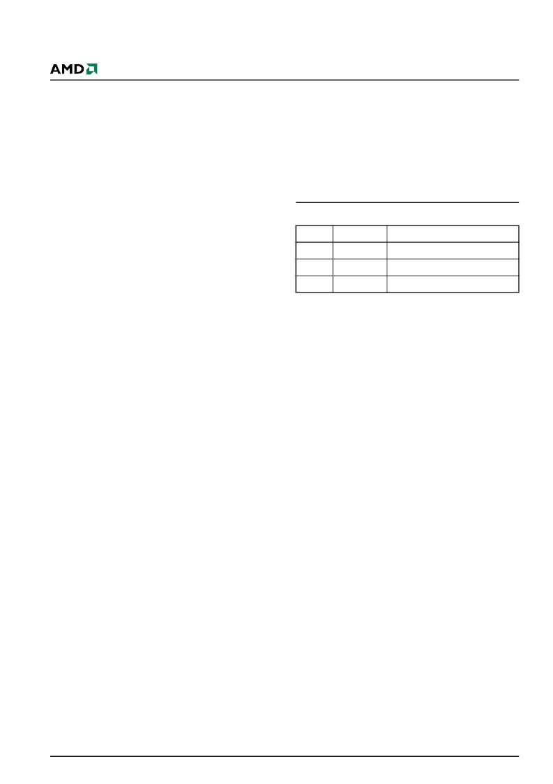
Table 2.
Burst Address Groups
As an example: if the starting address in the 8-word
mode is 39h, the address range to be read would be
38-3Fh, and the burst sequence would be
39-3A-3B-3C-3D-3E-3F-38h-etc. The burst sequence
begins with the starting address written to the device,
but wraps back to the first address in the selected
group. In a similar fashion, the 16-word and 32-word
Linear Wrap modes begin their burst sequence on the
starting address written to the device, and then wrap
back to the first address in the selected address group.
Note that in these three burst read modes the
address pointer does not cross the boundary that
occurs every 64 words; thus, no wait states are
inserted (except during the initial access).
The RDY pin indicates when data is valid on the bus.
The devices can wrap through a maximum of 128
words of data (8 words up to 16 times, 16 words up to
8 times, or 32 words up to 4 times) before requiring a
new synchronous access (latching of a new address).
Burst Suspend/Resume
The Burst Suspend/Resume feature allows the system
to temporarily suspend a synchronous burst operation
during the initial access (before data is available) or
after the device is outputting data. When the burst
operation is suspended, any previously latched internal
data and the current state are retained.
Burst Suspend requires CE# to be asserted, WE#
de-asserted, and the initial address latched by AVD# or
the CLK edge. Burst Suspend occurs when OE# is
de-asserted. See
Figure 21, “Reduced Wait-state
Handshake Burst Suspend/Resume at an Even
Address,” on page 61, Figure 22, “Reduced Wait-state
Handshake Burst Suspend/Resume at an Odd
Address,” on page 61, Figure 23, “Reduced Wait-state
Handshake Burst Suspend/Resume at Address 3Eh
(or Offset from 3Eh),” on page 62, Figure 24, “Reduced
Wait-state Handshake Burst Suspend/Resume at
Mode
Group Size
Group Address Ranges
8-word
8 words
0-7h, 8-Fh, 10-17h,...
16-word
16 words
0-Fh, 10-1Fh, 20-2Fh,...
32-word
32 words
00-1Fh, 20-3Fh, 40-5Fh,...
相關(guān)PDF資料 |
PDF描述 |
|---|---|
| AM29BDS128HE9VMI | 128 or 64 Megabit (8 M or 4 M x 16-Bit) CMOS 1.8 Volt-only Simultaneous Read/Write, Burst Mode Flash Memory |
| AM29BDS640H | 128 or 64 Megabit (8 M or 4 M x 16-Bit) CMOS 1.8 Volt-only Simultaneous Read/Write, Burst Mode Flash Memory |
| AM29BDS640HD8 | 128 or 64 Megabit (8 M or 4 M x 16-Bit) CMOS 1.8 Volt-only Simultaneous Read/Write, Burst Mode Flash Memory |
| AM29BDS640HD9 | 128 or 64 Megabit (8 M or 4 M x 16-Bit) CMOS 1.8 Volt-only Simultaneous Read/Write, Burst Mode Flash Memory |
| AM29BDS640HE8 | 128 or 64 Megabit (8 M or 4 M x 16-Bit) CMOS 1.8 Volt-only Simultaneous Read/Write, Burst Mode Flash Memory |
相關(guān)代理商/技術(shù)參數(shù) |
參數(shù)描述 |
|---|---|
| AM29BDS643GT5KVAI | 制造商:Spansion 功能描述:FLASH PARALLEL 1.8V 64MBIT 4MX16 55NS 44FBGA - Trays |
| AM29BL802CB-65RZET | 制造商:Spansion 功能描述: |
| AM29C01WW WAF | 制造商:Advanced Micro Devices 功能描述: |
| AM29C10API | 制造商:Rochester Electronics LLC 功能描述:- Bulk |
| AM29C10AWW DIE | 制造商:Advanced Micro Devices 功能描述: |
發(fā)布緊急采購,3分鐘左右您將得到回復。