- 您現(xiàn)在的位置:買賣IC網(wǎng) > PDF目錄362212 > ALD2721DB Operational Amplifier PDF資料下載
參數(shù)資料
| 型號: | ALD2721DB |
| 英文描述: | Operational Amplifier |
| 中文描述: | 運算放大器 |
| 文件頁數(shù): | 4/6頁 |
| 文件大小: | 46K |
| 代理商: | ALD2721DB |
ALD2704A/ALD2704B
ALD2704
Advanced Linear Devices
4
Design & Operating Notes:
1. The ALD2704 CMOS operational amplifier uses a 3 gain stage
architecture and an improved frequency compensation scheme to
achieve large voltage gain, high output driving capability, and better
frequency stability. The ALD2704 is internally compensated for unity
gain stability using a novel scheme. This design produces a clean
single pole roll off in the gain characteristics while providing for more
than 70 degrees of phase margin at the unity gain frequency. A unity
gain buffer using the ALD2704 will typically drive 400pF of external
load capacitance without stability problems. In the inverting unity gain
configuration, it can drive up to 800pF of load capacitance. Compared
to other CMOS operational amplifiers, the ALD2704 is much more
resistant to parasitic oscillations.
2. The ALD2704 has complementary p-channel and n-channel input
differential stages connected in parallel to accomplish rail to rail input
common mode voltage range. With the common mode input voltage
close to the power supplies, one of the two differential stages is
switched off internally. To maintain compatibility with other opera-
tional amplifiers, this switching point has been selected to be about
1.5V above the negative supply voltage. As offset voltage trimming
on the ALD2704 is made when the input voltage is symmetrical to the
supply voltages, this internal switching does not affect a large variety
of applications such as an inverting amplifier or non-inverting amplifier
with a gain greater than 2 (10V operation), where the common mode
voltage does not make excursions below this switching point.
3. The input bias and offset currents are essentially input protection
TYPICAL PERFORMANCE CHARACTERISTICS
diode reverse bias leakage currents, and are typically less than 1pA
at room temperature. This low input bias current assures that the
analog signal from the source will not be distorted by input bias
currents. For applications where source impedance is very high, it
may be necessary to limit noise and hum pickup through proper
shielding.
4. The output stage consists of class AB complementary output drivers,
capable of driving a low resistance load. The output voltage swing is
limited by the drain to source on-resistance of the output transistors as
determined by the bias circuitry, and the value of the load resistor. The
voltage follower configuration, the oscillation and resistant with the
rail- to-rail input and output feature, makes the ALD2704 an effective
analog signal buffer for medium to high source impedance sensors,
transducers, and other circuit networks.
5. The ALD2704 operational amplifier has been designed to provide
static discharge protection. Internally, the design has been carefully
implemented to minimize latch up. However, care must be exercised
when handling the device to avoid strong static fields. In using the
operational amplifier, the user is advised to power up the circuit before,
or simultaneously with, any input voltages applied and to limit input
voltages to not exceed 0.3V of the power supply voltage levels.
Alternatively, a 100K
or higher value resistor at the input terminals
will limit input currents to acceptable levels while causing very small
or negligible accuracy effects.
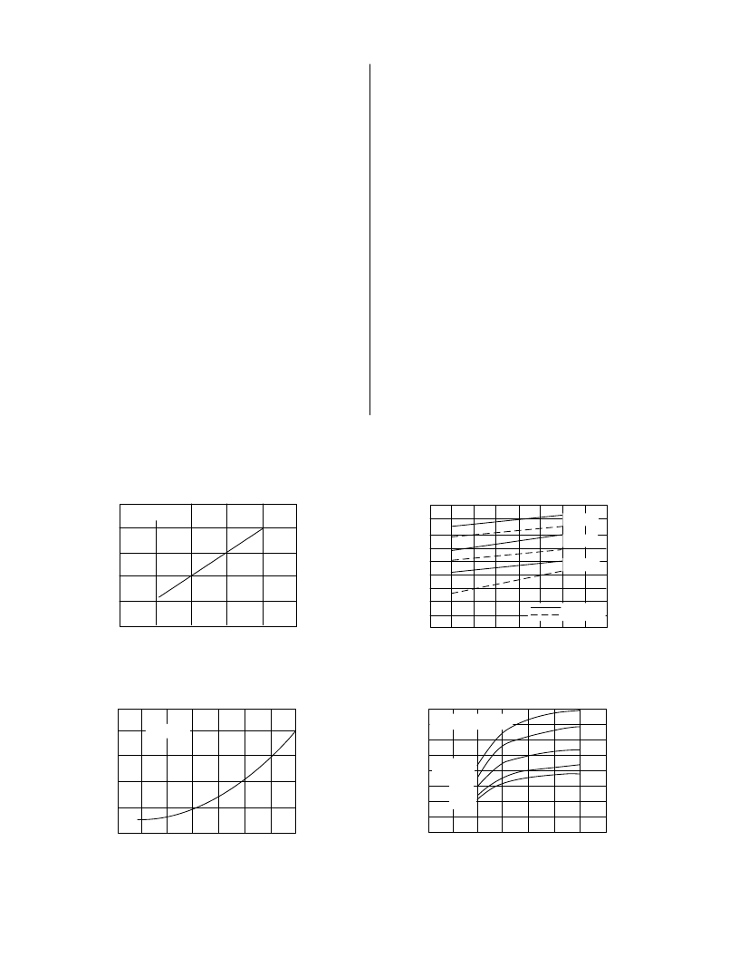
OPEN LOOP VOLTAGE GAIN AS A FUNCTION
OF SUPPLY VOLTAGE AND TEMPERATURE
1000
SUPPLY VOLTAGE (V)
100
10
1
O
G
0
±
2
±
4
±
6
R
L
= 5K
} -55
°
C
} +25
°
C
} +125
°
C
±
8
INPUT BIAS CURRENT AS A FUNCTION
OF AMBIENT TEMPERATURE
AMBIENT TEMPERATURE (
°
C)
1000
100
10
0.1
1.0
I
100
-25
0
75
125
50
25
-50
V
S
=
±
5.0V
10000
SUPPLY CURRENT AS A FUNCTION
OF SUPPLY VOLTAGE
SUPPLY VOLTAGE (V)
0
S
0
±
1
±
2
±
3
±
4
±
5
±
6
INPUTS GROUNDED
OUTPUT UNLOADED
+80
°
C
+125
°
C
+25
°
C
T
A
= -55
°
C
-25
°
C
±
7
1
2
3
4
5
6
7
8
COMMON MODE INPUT VOLTAGE RANGE
AS A FUNCTION OF SUPPLY VOLTAGE
SUPPLY VOLTAGE (V)
C
V
±
7
±
6
±
5
±
4
±
3
±
2
±
2
±
3
±
4
±
5
±
6
±
7
T
A
= 25
°
C
相關(guān)PDF資料 |
PDF描述 |
|---|---|
| ALD2721EDB | Operational Amplifier |
| ALD2721EPB | Operational Amplifier |
| ALD2721ESB | Operational Amplifier |
| ALD2721PB | Operational Amplifier |
| ALD2721SB | Operational Amplifier |
相關(guān)代理商/技術(shù)參數(shù) |
參數(shù)描述 |
|---|---|
| ALD2721E | 制造商:ALD 制造商全稱:Advanced Linear Devices 功能描述:DUAL EPAD?? MICROPOWER CMOS OPERATIONAL AMPLIFIER |
| ALD2721EDB | 制造商:未知廠家 制造商全稱:未知廠家 功能描述:Operational Amplifier |
| ALD2721EPB | 制造商:未知廠家 制造商全稱:未知廠家 功能描述:Operational Amplifier |
| ALD2721EPBL | 功能描述:運算放大器 - 運放 Op Amp, Micropower Dual Prec. EPAD RoHS:否 制造商:STMicroelectronics 通道數(shù)量:4 共模抑制比(最小值):63 dB 輸入補償電壓:1 mV 輸入偏流(最大值):10 pA 工作電源電壓:2.7 V to 5.5 V 安裝風(fēng)格:SMD/SMT 封裝 / 箱體:QFN-16 轉(zhuǎn)換速度:0.89 V/us 關(guān)閉:No 輸出電流:55 mA 最大工作溫度:+ 125 C 封裝:Reel |
| ALD2721ESB | 制造商:未知廠家 制造商全稱:未知廠家 功能描述:Operational Amplifier |
發(fā)布緊急采購,3分鐘左右您將得到回復(fù)。