- 您現(xiàn)在的位置:買賣IC網(wǎng) > PDF目錄362173 > AHF2815D-SLV Analog IC PDF資料下載
參數(shù)資料
| 型號: | AHF2815D-SLV |
| 英文描述: | Analog IC |
| 中文描述: | 模擬IC |
| 文件頁數(shù): | 5/9頁 |
| 文件大小: | 103K |
| 代理商: | AHF2815D-SLV |
5
AHE2815D
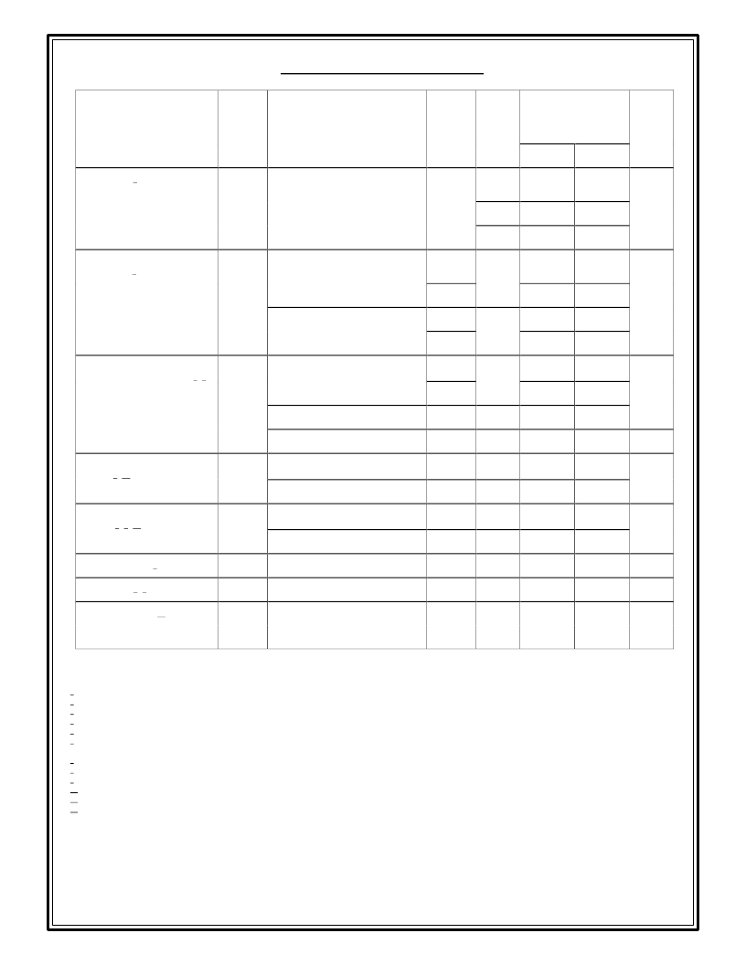
TABLE II. Electrical Performance Characteristics - Continued.
Test
Symbol
Conditions
-55
°
C
≤
T
C
≤
+125
°
C
V
IN
= 28 V dc ±5%, C
L
= 0 unless
otherwise specified
Group A
Subgroups
Device
Type
Limits
Unit
Min
Max
Switching 9/
frequency
F
S
I
OUT
= ±500 mA
4,5,6
01
225
275
KHz
02
225
245
03
250
275
Output response to step transient
load changes 7/
VO
TLOAD
50 percent load to/from 100 percent load
4
All
-300
+300
mV pk
5,6
-450
+450
No load to/from 50 percent load
4
All
-500
+500
5,6
-750
+750
Recovery time step transient load
changes transient load changes 1/ 7/
TT
LOAD
50 percent load to/from 100 percent load
4
All
70
μs
5,6
100
No load to 50 percent load
4,5,6
All
1500
50 percent load to no load
4,5,6
All
5
ms
Output response to transient step line
changes 5/ 12/
VO
TLINE
Input step 17 to 40 V dc
4,5,6
All
1500
mV pk
Input step 40 to 17 V dc
4,5,6
All
-1500
Recovery time transient step line
changes 1/ 5/ 12/
TT
LINE
Input step 17 to 40 V dc
4,5,6
All
4
ms
Input step 40 to 17 V dc
4,5,6
All
4
Turn on overshoot 9/
VTon
OS
I
OUT
= 0 and ±500 mA
4,5,6
All
600
mV pk
Turn on delay 2/ 9/
Ton
D
I
OUT
= 0 and ±500 mA
4,5,6
All
10
ms
Load fault recovery 12/
Tr
LF
4,5,6
All
10
ms
Notes:
1/ Recovery time is measured fromthe initiation of the transient to where V
OUT
has returned to within ±1 percent of V
OUT
at 50 percent load.
2/ Turn on delay time measurement is for either a step application of power at the input or the removal of a ground signal fromthe inhibit pin (pin 2) while power is applied to the input.
3/ An overload is that condition with a load in excess of the rated load but less than that necessary to trigger the short circuit protection and is the condition of maximumpower dissipation.
4/ Total power at both outputs. For operation at 16 V dc input, derate output power by 33 percent.
5/ Input step transition time between 2 and 10 mcroseconds.
6/ Capacitive load may be any value from0 to the maximumlimt without compromsing dc performance. A capacitive load in excess of the maximumlimt will not disturb loop stability but may
interfere with the operation of the load fault detection circuitry, appearing as a short circuit during turn on.
7/ Load step transition time between 2 and 10 mcroseconds.
8/ Bandwidth guaranteed by design. Tested for 20 KHz to 2 MHz.
9/ Tested at each output.
10/ When operating with unbalanced loads, at least 25 percent of the load must be on the positive output to maintain regulation.
11/ Parameter guaranteed by line and load regulation tests.
12/ Parameter shall be tested as part of design characterization and after design or process changes. Thereafter parameters shall be guaranteed to the limts specified in Table II.
相關(guān)PDF資料 |
PDF描述 |
|---|---|
| AHF2815T | Hi-Rel DC-DC Standard Triple Converter in a AHF package |
| AHF2812DF-MSTR | Analog IC |
| AHF2812DF-SLV | Analog IC |
| AHF2812D-MSTR | Analog IC |
| AHF2812D-SLV | Analog IC |
相關(guān)代理商/技術(shù)參數(shù) |
參數(shù)描述 |
|---|---|
| AHF2815S | 制造商:International Rectifier 功能描述:DC/DC CONVERTER, MINIMUM SCREENING - Bulk |
| AHF2815S/CH | 制造商:International Rectifier 功能描述:Module DC-DC 1-OUT 15V 2A 12W 8-Pin AHF 制造商:International Rectifier 功能描述:DC/DC CONVERTER, CLASS H - Bulk |
| AHF2815S/ES | 制造商:International Rectifier 功能描述:Module DC-DC 1-OUT 15V 2A 12W 8-Pin AHF 制造商:International Rectifier 功能描述:DC/DC CONVERTER, ENVIRONMENTAL SCREENING - Bulk |
| AHF2815S/HB | 制造商:International Rectifier 功能描述:DC/DC CONVERTER, CLASS H EQUIVALENT, NO ELEM EVAL - Bulk |
| AHF2815SF | 制造商:International Rectifier 功能描述:DC/DC CONVERTER, FLANGED, MINIMUM SCREENING - Bulk |
發(fā)布緊急采購,3分鐘左右您將得到回復(fù)。