- 您現(xiàn)在的位置:買賣IC網(wǎng) > PDF目錄378298 > AHF2812S (International Rectifier) 28V Input, Single and Dual Output PDF資料下載
參數(shù)資料
| 型號(hào): | AHF2812S |
| 廠商: | International Rectifier |
| 英文描述: | 28V Input, Single and Dual Output |
| 中文描述: | 28V輸入,單路和雙路輸出 |
| 文件頁(yè)數(shù): | 11/17頁(yè) |
| 文件大?。?/td> | 148K |
| 代理商: | AHF2812S |
第1頁(yè)第2頁(yè)第3頁(yè)第4頁(yè)第5頁(yè)第6頁(yè)第7頁(yè)第8頁(yè)第9頁(yè)第10頁(yè)當(dāng)前第11頁(yè)第12頁(yè)第13頁(yè)第14頁(yè)第15頁(yè)第16頁(yè)第17頁(yè)
www.irf.com
11
AHF28XX Series
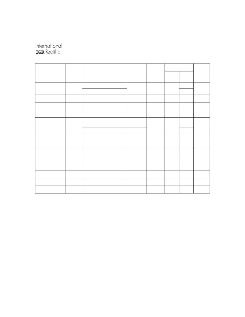
Table V. Electrical Performance Characteristics -
continued
AHF2812D
Notes to Specifications
1. Parameter guaranteed by line load and cross regulation tests.
2. Up to 90 percent of full power is available from either output provided the total output does not exceed 12W.
3. Bandwidth guaranteed by design. Tested for 20 kHz to 2 MHz.
4. Load current split equally between +V
and –V
.
5. 1.2 watt load on output under test, 1.2 watt to 10.8 watt load change on other output.
6. Capacitive load may be any value from 0 to the maximum limit without compromising dc performance.
A capacitive oad in excess of the maximum limit will not disturb loop stability but may interfere with the
operation of the load fault detection circuitry, appearing as a short circuit during turn-on.
7. Parameter shall be tested as part of design characterization and after design or process changes.
Thereafter, parameters shall be guaranteed to the limits specified in Table V.
8. An overload is that condition with a load in excess of the rated load but less than that necessary to
trigger the short circuit protection and is the condition of maximum power dissipation.
9. Load step transition time between 2 and 10 microseconds.
10. Recovery time is measured from the initiation of the transient to where V
OUT
has returned to within ±1
percent of V
at 50 percent load.
11. Input step transition time between 2 and 10 microseconds.
12. Turn-on delay time measurement is for either a step application of power at the input or the removal of
a ground signal from the inhibit pin (pin 1) while power is applied to the input.
Limits
Test
Symbol
Conditions
-55°C
≤
Tc
≤
+125°C
Vin = 28 Vdc ±5%, C
= 0
unless otherwise specified
Overload, T
C
= +25°C
Short circuit, T
C
= +25°C
Group A
Subgroups
Device
Types
Min
Max
Unit
8
6
Power dissipa-
tion load fault
P
D
1,2,3
01
2
W
Switching
frequency
Output response
to step transient
load changes
4
F
S
I
= 1000mA
500 mA to/from 1000mA
4,5,6
4,5,6
01
01
01
500
-200
-800
600
+200
+800
kHz
mV pk
4,9
VO
TLOAD
0 mA to/from 500 mA
4,5,6
500 mA to/from 1000mA
4,5,6
70
Recovery time
step transient load
changes
Output response
transient step line
changes
Recovery time
transient step line
changes
4,9,10
TT
LOAD
0 mA to/from 500 mA
4,5,6
1000
μs
4,7,11
VO
TLINE
Input step from/to 16 to
40 V dc, I
OUT
=1000mA
4,5,6
01
-750
+750
mV pk
4,7,10,11
TT
LINE
Input step from/to 16 to 40 V
dc, I
OUT
=1000mA
4,5,6
01
1200
μs
Turn on
overshoot
Turn on delay
Load fault
recovery
Weight
4
VTon
OS
Ton
D
I
OUT
=0 and 1000mA
4,5,6
01
600
mV pk
4,12
I
OUT
= 0 and 1000mA
4,5,6
01
25
ms
7
Tr
LF
4,5,6
01
25
38
ms
grams
相關(guān)PDF資料 |
PDF描述 |
|---|---|
| AHF2812SF | 28V Input, Single and Dual Output |
| AHF2815D | 28V Input, Single and Dual Output |
| AHF2815DF | 28V Input, Single and Dual Output |
| AHF2815S | 28V Input, Single and Dual Output |
| AHF2815SF | 28V Input, Single and Dual Output |
相關(guān)代理商/技術(shù)參數(shù) |
參數(shù)描述 |
|---|---|
| AHF2812S/CH | 制造商:International Rectifier 功能描述:DC/DC CONVERTER, CLASS H - Bulk |
| AHF2812S/ES | 制造商:International Rectifier 功能描述:DC/DC CONVERTER, ENVIRONMENTAL SCREENING - Bulk |
| AHF2812S/HB | 制造商:International Rectifier 功能描述:DC/DC CONVERTER, CLASS H EQUIVALENT, NO ELEM EVAL - Bulk |
| AHF2812SF | 制造商:International Rectifier 功能描述:DC/DC CONVERTER, FLANGED, MINIMUM SCREENING - Bulk |
| AHF2812SF/CH | 制造商:International Rectifier 功能描述:DC/DC CONVERTER, FLANGED, CLASS H - Bulk |
發(fā)布緊急采購(gòu),3分鐘左右您將得到回復(fù)。