- 您現(xiàn)在的位置:買賣IC網(wǎng) > PDF目錄235794 > AGLE600V2-FFGG484C FPGA, 13824 CLBS, 600000 GATES, PBGA256 PDF資料下載
參數(shù)資料
| 型號: | AGLE600V2-FFGG484C |
| 元件分類: | FPGA |
| 英文描述: | FPGA, 13824 CLBS, 600000 GATES, PBGA256 |
| 封裝: | 17 X 17 MM, 1.60 MM HEIGHT, 1 MM PITCH, ROHS COMPLIANT, FBGA-256 |
| 文件頁數(shù): | 9/156頁 |
| 文件大小: | 5023K |
| 代理商: | AGLE600V2-FFGG484C |
第1頁第2頁第3頁第4頁第5頁第6頁第7頁第8頁當(dāng)前第9頁第10頁第11頁第12頁第13頁第14頁第15頁第16頁第17頁第18頁第19頁第20頁第21頁第22頁第23頁第24頁第25頁第26頁第27頁第28頁第29頁第30頁第31頁第32頁第33頁第34頁第35頁第36頁第37頁第38頁第39頁第40頁第41頁第42頁第43頁第44頁第45頁第46頁第47頁第48頁第49頁第50頁第51頁第52頁第53頁第54頁第55頁第56頁第57頁第58頁第59頁第60頁第61頁第62頁第63頁第64頁第65頁第66頁第67頁第68頁第69頁第70頁第71頁第72頁第73頁第74頁第75頁第76頁第77頁第78頁第79頁第80頁第81頁第82頁第83頁第84頁第85頁第86頁第87頁第88頁第89頁第90頁第91頁第92頁第93頁第94頁第95頁第96頁第97頁第98頁第99頁第100頁第101頁第102頁第103頁第104頁第105頁第106頁第107頁第108頁第109頁第110頁第111頁第112頁第113頁第114頁第115頁第116頁第117頁第118頁第119頁第120頁第121頁第122頁第123頁第124頁第125頁第126頁第127頁第128頁第129頁第130頁第131頁第132頁第133頁第134頁第135頁第136頁第137頁第138頁第139頁第140頁第141頁第142頁第143頁第144頁第145頁第146頁第147頁第148頁第149頁第150頁第151頁第152頁第153頁第154頁第155頁第156頁
IGLOOe DC and Switching Characteristics
2- 92
Advance v0.3
Clock Conditioning Circuits
CCC Electrical Specifications
Timing Characteristics
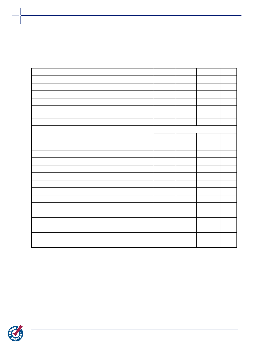
Table 2-135 IGLOOe CCC/PLL Specification
For IGLOOe V2 or V5 Devices, 1.5 V DC Core Supply Voltage
Parameter
Min.
Typ.
Max.
Units
Clock Conditioning Circuitry Input Frequency fIN_CCC
1.5
250
MHz
Clock Conditioning Circuitry Output Frequency fOUT_CCC
0.75
250
MHz
Serial Clock (SCLK) for Dynamic PLL3
100
ps
Delay Increments in Programmable Delay Blocks1, 2
360
Number of Programmable Values in Each Programmable Delay
Block
32
ns
Input Cycle-to-Cycle Jitter (peak magnitude)
1
CCC Output Peak-to-Peak Period Jitter FCCC_OUT
Max Peak-to-Peak Period Jitter
1 Global
Network
Used
External
FB Used
3 Global
Networks
Used
0.75 MHz to 24 MHz
0.50%
0.75%
0.70%
24 MHz to 100 MHz
1.00%
1.50%
1.20%
100 MHz to 250 MHz
2.50%
3.75%
2.75%
Acquisition Time
LockControl = 0
300
s
LockControl = 1
6.0
ms
Tracking Jitter
LockControl = 0
2.5
ns
LockControl = 1
1.5
ns
Output Duty Cycle
48.5
51.5
%
Delay Range in Block: Programmable Delay 1 1, 2, 4
1.25
15.65
ns
Delay Range in Block: Programmable Delay 2 1, 2, 4
0.025
15.65
ns
Delay Range in Block: Fixed Delay 1, 2
3.5
ns
Notes:
1. This delay is a function of voltage and temperature. See Table 2-6 on page 2-6 and Table 2-7 on page 2-6
for deratings.
2. TJ = 25°C, VCC = 1.5 V
3. Maximum value obtained for a Std. speed grade device in Worst Case Commercial Conditions.For specific
junction temperature and voltage supply levels, refer to Table 2-6 on page 2-6 for derating values.
4. For definitions of Type 1 and Type 2, refer to the PLL Block Diagram in the Clock Conditioning Circuits in
IGLOO and ProASIC3 Devices chapter of the handbook.
5. Tracking jitter is defined as the variation in clock edge position of PLL outputs with reference to the PLL
input clock edge. Tracking jitter does not measure the variation in PLL output period, which is covered by
the period jitter parameter.
相關(guān)PDF資料 |
PDF描述 |
|---|---|
| AGLE600V2-FG256C | FPGA, 13824 CLBS, 600000 GATES, PBGA256 |
| AGLE600V2-FGG256C | FPGA, 13824 CLBS, 600000 GATES, PBGA256 |
| AGLE600V2-FGG484C | FPGA, 13824 CLBS, 600000 GATES, PBGA256 |
| AGLE600V5-FFG256C | FPGA, 13824 CLBS, 600000 GATES, PBGA256 |
| AGLE600V5-FFG484C | FPGA, 13824 CLBS, 600000 GATES, PBGA256 |
相關(guān)代理商/技術(shù)參數(shù) |
參數(shù)描述 |
|---|---|
| AGLE600V2-FFGG896 | 制造商:ACTEL 制造商全稱:Actel Corporation 功能描述:IGLOOe Low-Power Flash FPGAs with Flash Freeze Technology |
| AGLE600V2-FFGG896ES | 制造商:ACTEL 制造商全稱:Actel Corporation 功能描述:IGLOOe Low-Power Flash FPGAs with Flash Freeze Technology |
| AGLE600V2-FFGG896I | 制造商:ACTEL 制造商全稱:Actel Corporation 功能描述:IGLOOe Low-Power Flash FPGAs with Flash Freeze Technology |
| AGLE600V2-FFGG896PP | 制造商:ACTEL 制造商全稱:Actel Corporation 功能描述:IGLOOe Low-Power Flash FPGAs with Flash Freeze Technology |
| AGLE600V2-FG256 | 功能描述:IC FPGA 1KB FLASH 600K 256-FBGA RoHS:否 類別:集成電路 (IC) >> 嵌入式 - FPGA(現(xiàn)場可編程門陣列) 系列:IGLOOe 標(biāo)準(zhǔn)包裝:40 系列:SX-A LAB/CLB數(shù):6036 邏輯元件/單元數(shù):- RAM 位總計:- 輸入/輸出數(shù):360 門數(shù):108000 電源電壓:2.25 V ~ 5.25 V 安裝類型:表面貼裝 工作溫度:0°C ~ 70°C 封裝/外殼:484-BGA 供應(yīng)商設(shè)備封裝:484-FPBGA(27X27) |
發(fā)布緊急采購,3分鐘左右您將得到回復(fù)。