- 您現(xiàn)在的位置:買賣IC網(wǎng) > PDF目錄374048 > ADXL190 (Analog Devices, Inc.) Circular Connector; No. of Contacts:3; Series:LJTP02R; Body Material:Aluminum; Connecting Termination:Crimp; Connector Shell Size:9; Circular Contact Gender:Pin; Circular Shell Style:Box Mount Receptacle; Insert Arrangement:9-98 PDF資料下載
參數(shù)資料
| 型號: | ADXL190 |
| 廠商: | Analog Devices, Inc. |
| 元件分類: | 圓形連接器 |
| 英文描述: | Circular Connector; No. of Contacts:3; Series:LJTP02R; Body Material:Aluminum; Connecting Termination:Crimp; Connector Shell Size:9; Circular Contact Gender:Pin; Circular Shell Style:Box Mount Receptacle; Insert Arrangement:9-98 |
| 中文描述: | 低成本-100 gSingle軸加速度計的模擬輸出 |
| 文件頁數(shù): | 4/5頁 |
| 文件大小: | 98K |
| 代理商: | ADXL190 |
REV. 0
ADXL190
–4–
APPLICATIONS
All the circuitry needed to drive the sensor and convert the
capacitance change to voltage is incorporated on-chip requiring
no external components except for standard power supply de-
coupling. Both sensitivity and the zero-
g
value are ratiometric to
the supply voltage, so that ratiometric devices following the
accelerometer (such as an ADC, etc.) will track the accelerom-
eter if the supply voltage changes. The output voltage (V
OUT
) is
a function of both the acceleration input (a) and the power
supply voltage (V
S
) as follows:
V
OUT
=
V
S
/2 – (
Sensitivity
×
V
S
/
5
V
×
a
)
Adjusting the 0
g
Bias Level
In some cases the user may have an asymmetrical input or may
want to fine adjust the zero-
g
output level to obtain maximum
dynamic range. The zero-
g
level is adjusted by supplying a
voltage to the zero-
g
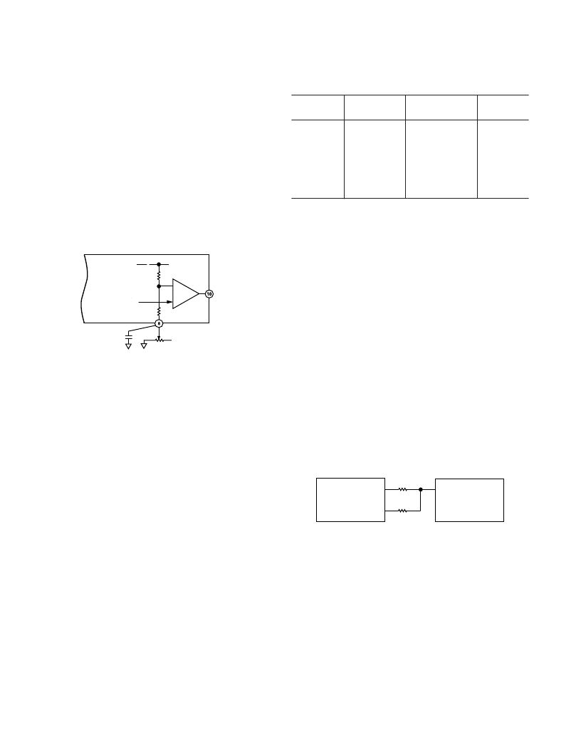
adjustment pin (see Figure 2).
+V
S
2
25k
V
5k
V
ADXL190
ZERO g ADJUST
+V
S
200k
V
FILTER
V
OUT
GAIN = 3
ACCELERATION
SIGNAL
C2
0.1
m
F
Figure 2. Optional Zero-g Adjust Circuit Detail
Any voltage difference between the zero-
g
adjustment pin and
V
S
/2 is reduced by a factor of 6 by the internal resistor divider.
This is then gained by the factor of 3 in the output stage for a
total gain of 0.5 for the zero-
g
adjustment. (Note: The ratio of
the resistors in the divider is consistent from part-to-part; how-
ever, the absolute values can have a
±
30% tolerance). The
zero-
g
adjustment voltage can be set up by a variety of methods
including a potentiometer (as shown in Figure 2), a PWM sig-
nal, or with a simple three-state output.
The simplest way is by adding a resistor between the ZERO
g
ADJUST pin and V
S
or ground. The output will be offset by:
Offset
(
V
) = (7.5
×
V
S
)/(30 +
R
)
where
R
is in k
and connected to
V
S
.
Offset
(
V
) = (–7.5
×
V
S
)/(30 +
R
)
where
R
is in k
and connected to ground.
Resistors may also be connected to microcontroller I/O pins as
shown in Figure 3. Using two I/Os that may be set to V
S
, ground,
or three-state, there are seven possibilities as shown in Table I
(one cannot set one I/O pin to V
S
and the other to ground).
Using such a system, any ADXL190 may be user trimmed to
output 2.5 V
±
35 mV at zero
g
.
Table I. Offsets Produced Using the Circuit in Figure 3 for V
S
= 5 V
Offset Voltage
Produced
P1
P0
Offset in
g
Three-State
Three-State
0
0
Three-State
1
1
Three-State
0
Three-State
0
1
Three-State
1
0 mV
–71 mV
–134 mV
–191 mV
71 mV
134 mV
191 mV
0
–4
–7.4
–10.6
4
7.4
10.6
Another way to adjust the zero
g
offset is to supply a voltage to
the ZERO
g
ADJUST pin. The difference between V
S
/2 and
the voltage at the ZERO
g
ADJUST pin is reduced by a factor
of 6 (as a result of the internal 5 k
and 25 k
voltage divider)
and then multiplied by a factor of 3 in the output stage of the
ADXL190 resulting in a total gain of 0.5. Offset is thus de-
scribed by the following equation:
Offset
(
V
) = (
Voltage at the ZERO g AD
J
UST Pin
–
V
S
/2)/2
This voltage may be produced by a variety of methods includ-
ing a PWM signal from a microcontroller. Care must be taken
that the output impedance of this voltage source is less than
5 k
and that there is very little ripple (noise). Any noise at the
ZERO
g
ADJUST pin will cause output errors.
If an asymmetric range of acceleration is required (e.g., +75
g
to –125
g
) a resistor may be connected between the ZERO
g
ADJUST and ground or V
S
as described above. For example:
For a range of +75
g
to –125
g
the offset required is –25
g
.
–25
g
at 18 mV/
g
= 450 mV of offset is required.
Rearranging the offset equations above:
R
= [(7.5
×
V
S
)/
offset
] –30 = 53.3
k
connected to ground.
For asymmetric operation the
g
range midpoint may be shifted
up to
±
80
g
typically.
500k
V
250k
V
ZERO g
ADJUST
ADXL190
MICROCONTROLLER
P1
P0
Figure 3. An Offset Adjustment Scheme
相關PDF資料 |
PDF描述 |
|---|---|
| ADXL190WQC | Circular Connector; No. of Contacts:22; Series:LJTPQ00R; Body Material:Aluminum; Connecting Termination:Crimp; Connector Shell Size:13; Circular Contact Gender:Socket; Circular Shell Style:Wall Mount Receptacle |
| ADXL190* | Low Cost 6100 gSingle Axis Accelerometer with Analog Output |
| ADXL202E | Circular Connector; MIL SPEC:MIL-DTL-38999 Series I; Body Material:Metal; Series:LJT; No. of Contacts:11; Connector Shell Size:19; Connecting Termination:Crimp; Circular Shell Style:Wall Mount Receptacle; Body Style:Straight RoHS Compliant: No |
| ADXL202 | Circular Connector; No. of Contacts:37; Series:LJTPQ00R; Body Material:Aluminum; Connecting Termination:Crimp; Connector Shell Size:15; Circular Contact Gender:Pin; Circular Shell Style:Wall Mount Receptacle |
| ADXL202AE | Circular Connector; MIL SPEC:MIL-DTL-38999 Series I; Body Material:Metal; Series:LJT; No. of Contacts:5; Connector Shell Size:15; Connecting Termination:Crimp; Circular Shell Style:Wall Mount Receptacle; Body Style:Straight RoHS Compliant: No |
相關代理商/技術參數(shù) |
參數(shù)描述 |
|---|---|
| ADXL190EM-1 | 制造商:AD 制造商全稱:Analog Devices 功能描述:ADXL105/ADXL150/ADXL250/ADXL190 Evaluation Modules |
| ADXL190WQC | 制造商:Analog Devices 功能描述: 制造商:Analog Devices 功能描述:SENSOR ((NW)) |
| ADXL193 | 制造商:AD 制造商全稱:Analog Devices 功能描述:Single-Axis, High-g, iMEMS Accelerometers |
| ADXL193-MISC | 功能描述:ACCELEROMETER CLCC 制造商:analog devices inc. 系列:iMEMS? 零件狀態(tài):停產(chǎn) 類型:模擬 軸:X 加速度范圍:- 靈敏度(LSB/g):- 靈敏度(mV/g):- 帶寬:400Hz 輸出類型:模擬電壓 電壓 - 電源:4.75 V ~ 5.25 V 特性:- 工作溫度:-40°C ~ 125°C(TA) 安裝類型:表面貼裝 標準包裝:1 |
發(fā)布緊急采購,3分鐘左右您將得到回復。