- 您現(xiàn)在的位置:買賣IC網(wǎng) > PDF目錄374046 > ADV7176AKS (ANALOG DEVICES INC) High Quality, 10-Bit, Digital CCIR-601 to PAL/NTSC Video Encoder PDF資料下載
參數(shù)資料
| 型號: | ADV7176AKS |
| 廠商: | ANALOG DEVICES INC |
| 元件分類: | 顏色信號轉(zhuǎn)換 |
| 英文描述: | High Quality, 10-Bit, Digital CCIR-601 to PAL/NTSC Video Encoder |
| 中文描述: | COLOR SIGNAL ENCODER, PQFP44 |
| 封裝: | PLASTIC, MQFP-44 |
| 文件頁數(shù): | 21/52頁 |
| 文件大小: | 629K |
| 代理商: | ADV7176AKS |
第1頁第2頁第3頁第4頁第5頁第6頁第7頁第8頁第9頁第10頁第11頁第12頁第13頁第14頁第15頁第16頁第17頁第18頁第19頁第20頁當前第21頁第22頁第23頁第24頁第25頁第26頁第27頁第28頁第29頁第30頁第31頁第32頁第33頁第34頁第35頁第36頁第37頁第38頁第39頁第40頁第41頁第42頁第43頁第44頁第45頁第46頁第47頁第48頁第49頁第50頁第51頁第52頁
ADV7175A/ADV7176A
–21–
REV. B
OUT PUT VIDE O T IMING
T he video timing generator generates the appropriate SYNC,
BLANK
and BURST sequence that controls the output analog
waveforms. T hese sequences are summarized below. In slave
modes, the following sequences are synchronized with the input
timing control signals. In master modes, the timing generator
free runs and generates the following sequences in addition to
the output timing control signals.
NT SC–Interlaced:
Scan Lines 1–9 and 264–272 are always
blanked and vertical sync pulses are included. Scan Lines 525,
10–21 and 262, 263, 273–284 are also blanked and can be used
for closed captioning data. Burst is disabled on lines 1–6, 261–
269 and 523–525.
NT SC–Noninterlaced:
Scan Lines 1–9 are always blanked,
and vertical sync pulses are included. Scan Lines 10–21 are also
blanked and can be used for closed captioning data. Burst is
disabled on Lines 1–6, 261–262.
PAL–Interlaced:
Scan Lines 1–6, 311–318 and 624–625 are
always blanked, and vertical sync pulses are included in Fields
1, 2, 5 and 6. Scan Lines 1–5, 311–319 and 624–625 are al-
ways blanked, and vertical sync pulses are included in Fields 3,
4, 7 and 8. T he remaining scan lines in the vertical blanking
interval are also blanked and can be used for teletext data.
Burst is disabled on Lines 1–6, 311–318 and 623–625 in Fields
1, 2, 5 and 6. Burst is disabled on Lines 1–5, 311–319 and
623–625 in Fields 3, 4, 7 and 8.
PAL–Noninterlaced:
Scan Lines 1–6 and 311–312 are always
blanked, and vertical sync pulses are included. T he remaining
scan lines in the vertical blanking interval are also blanked and
can be used for teletext data. Burst is disabled on Lines 1–5,
310–312.
POWE R-ON RE SE T
After power-up, it is necessary to execute a reset operation. A
reset occurs on the falling edge of a high-to-low transition on
the
RESET
pin. T his initializes the pixel port so that the
pixel inputs, P7–P0 are selected. After reset, the ADV7175A/
ADV7176A is automatically set up to operate in NT SC mode.
Subcarrier frequency code 21F07C16HEX is loaded into the
subcarrier frequency registers. All other registers, with the
exception of Mode Register 0, are set to 00H. All bits in Mode
Register 0 are set to Logic Level “0” except Bit MR02. Bit
MR02 of Mode Register 0 is set to Logic “1.” T his enables the
7.5 IRE pedestal.
SCH Phase Mode
T he SCH phase is configured in default mode to reset every
four (NT SC) or eight (PAL) fields to avoid an accumulation of
SCH phase error over time. In an ideal system, zero SCH phase
error would be maintained forever, but in reality, this is impos-
sible to achieve due to clock frequency variations. T his effect is
reduced by the use of a 32-bit DDS, which generates this SCH.
Resetting the SCH phase every four or eight fields avoids the
accumulation of SCH phase error, and results in very minor
SCH phase jumps at the start of the four or eight field sequence.
Resetting the SCH phase should not be done if the video source
does not have stable timing or the ADV7175A/ADV7176A is
configured in RT C mode (MR21 = 1 and MR22 = 1). Under
these conditions (unstable video) the subcarrier phase reset
should be enabled MR22 = 0 and MR21 = 1) but no reset
applied. In this configuration the SCH phase will never be reset,
which means that the output video will now track the unstable
input video. T he subcarrier phase reset, when applied, will reset
the SCH phase to Field 0 at the start of the next field (e.g.,
subcarrier phase reset applied in Field 5 [PAL] on the start of
the next field SCH phase will be reset to Field 0).
MPU PORT DE SCRIPT ION
T he ADV7175A and ADV7176A support a two-wire serial (I
2
C
Compatible) microprocessor bus driving multiple peripherals.
T wo inputs, serial data (SDAT A) and serial clock (SCLOCK ),
carry information between any device connected to the bus.
Each slave device is recognized by a unique address. T he
ADV7175A and ADV7176A each have four possible slave
addresses for both read and write operations. T hese are unique
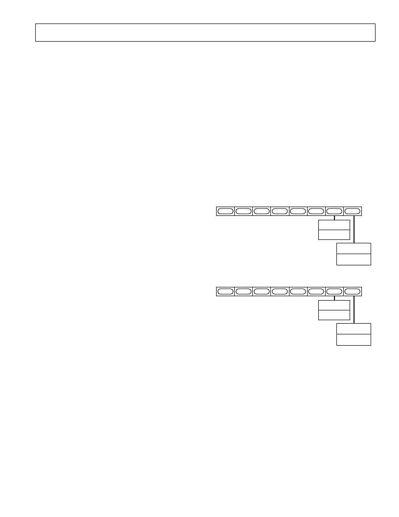
addresses for each device and are illustrated in Figure 27 and
Figure 28. T he LSB sets either a read or write operation. Logic
Level “1” corresponds to a read operation, while Logic Level
“0” corresponds to a write operation. A1 is set by setting the
ALSB pin of the ADV7175A/ADV7176A to Logic Level “0” or
Logic Level “1.”
1
X
1
0
1
0
1
A1
ADDRESS
CONTROL
SET UP BY
ALSB
READ/WRITE
CONTROL
0
1
WRITE
READ
Figure 27. ADV7175A Slave Address
0
X
1
0
1
0
1
A1
ADDRESS
CONTROL
SET UP BY
ALSB
READ/WRITE
CONTROL
0
1
WRITE
READ
Figure 28. ADV7176A Slave Address
T o control the various devices on the bus, the following proto-
col must be followed: First, the master initiates a data transfer by
establishing a start condition, defined by a high-to-low transition
on SDAT A while SCLOCK remains high. T his indicates that
an address/data stream will follow. All peripherals respond to
the start condition and shift the next eight bits (7-bit address +
R/
W
bit). T he bits transfer from MSB down to LSB. T he pe-
ripheral that recognizes the transmitted address responds by
pulling the data line low during the ninth clock pulse. T his is
known as an acknowledge bit. All other devices withdraw from
the bus at this point and maintain an idle condition. T he idle
condition is where the device monitors the SDAT A and SCLOCK
lines waiting for the start condition and the correct transmitted
address. T he R/
W
bit determines the direction of the data. A
Logic “0” on the LSB of the first byte means that the master
will write information to the peripheral. A Logic “1” on the
LSB of the first byte means that the master will read informa-
tion from the peripheral.
相關(guān)PDF資料 |
PDF描述 |
|---|---|
| ADV7176A* | High Quality. 10-Bit. Digital CCIR-601 to PAL/NTSC Video Encoder |
| ADV7175 | Integrated Digital CCIR-601 YCrCb to PAL/NTSC Video Encoder |
| ADV7175KS | Integrated Digital CCIR-601 YCrCb to PAL/NTSC Video Encoder |
| ADV7176 | Integrated Digital CCIR-601 YCrCb to PAL/NTSC Video Encoder |
| ADV7176KS | Integrated Digital CCIR-601 YCrCb to PAL/NTSC Video Encoder |
相關(guān)代理商/技術(shù)參數(shù) |
參數(shù)描述 |
|---|---|
| ADV7176AKSZ | 制造商:Analog Devices 功能描述:Video Encoder 4DAC 10-Bit 44-Pin MQFP 制造商:Analog Devices 功能描述:IC VIDEO ENCODER |
| ADV7176KS | 制造商:AD 制造商全稱:Analog Devices 功能描述:Integrated Digital CCIR-601 YCrCb to PAL/NTSC Video Encoder |
| ADV7177 | 制造商:AD 制造商全稱:Analog Devices 功能描述:Integrated Digital CCIR-601 to PAL/NTSC Video Encoder |
| ADV7177KS | 制造商:Analog Devices 功能描述:Video Encoder 3DAC 9-Bit 44-Pin MQFP 制造商:Rochester Electronics LLC 功能描述:NTSC/PAL 3 DAC VIDEO ENCODER I.C. - Bulk 制造商:Analog Devices 功能描述:IC VIDEO ENCODER |
| ADV7177KS-REEL | 制造商:Analog Devices 功能描述:Video Encoder 3DAC 9-Bit 44-Pin MQFP T/R 制造商:Rochester Electronics LLC 功能描述:NTSC/PAL 3 DAC VIDEO ENCODER I.C. - Tape and Reel |
發(fā)布緊急采購,3分鐘左右您將得到回復(fù)。