- 您現(xiàn)在的位置:買賣IC網(wǎng) > PDF目錄1900 > ADSP-BF526KBCZ-4C2 (Analog Devices Inc)IC DSP CTRLR 400MHZ 289CSPBGA PDF資料下載
第1頁(yè)第2頁(yè)第3頁(yè)第4頁(yè)第5頁(yè)第6頁(yè)第7頁(yè)第8頁(yè)第9頁(yè)第10頁(yè)第11頁(yè)第12頁(yè)第13頁(yè)第14頁(yè)第15頁(yè)第16頁(yè)第17頁(yè)第18頁(yè)第19頁(yè)第20頁(yè)第21頁(yè)第22頁(yè)第23頁(yè)第24頁(yè)第25頁(yè)第26頁(yè)第27頁(yè)第28頁(yè)第29頁(yè)第30頁(yè)第31頁(yè)第32頁(yè)當(dāng)前第33頁(yè)第34頁(yè)第35頁(yè)第36頁(yè)
Rev. A
|
Page 6 of 36
|
March 2010
ADSP-BF522C/ADSP-BF523C/ADSP-BF524C/ADSP-BF525C/ADSP-BF526C/ADSP-BF527C
The programmer can simultaneously load the volume control of
both channels by writing to the LRHPBOTH (Register R2, Bit
D8) and RLHPBOTH (Register R3, Bit D8) bits of the left- or
right-channel DAC volume registers.
The maximum output level of the headphone outputs is
1.0 V rms when AVDD and HPVDD = 3.3 V. To suppress audi-
ble pops and clicks, the headphone and line outputs are held at
the VMID dc voltage level when the device is set to standby
mode or when the headphone outputs are muted.
The stereo line outputs of the codec, the LOUT and ROUT pins,
can drive a load impedance of 10 k
Ω and 50 pF. The line output
signal levels are not adjustable at the output mixer, which has a
fixed gain of 0 dB. The maximum output level of the line out-
puts is 1.0 V rms when AVDD = 3.3 V.
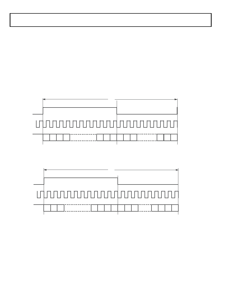
DIGITAL AUDIO INTERFACE
The digital audio input can support the following digital audio
communication protocols: right-justified mode, left-justified
through Figure 10 on Page 7.
The mode selection is performed by writing to the FORMAT
bits of the digital audio interface register (Register R7, Bit D1
and Bit D0). All modes are MSB first and operate with data of 16
to 32 bits.
Figure 6. Left-Justified Audio Input Mode
Figure 7. Right-Justified Audio Input Mode
ADCLRC/
DACLRC
CODEC_BCLK
ADCDAT/
DACDAT
1234
N
X
N
12
LEFT CHANNEL
3
RIGHT CHANNEL
1/
fS
X = DON’T CARE.
ADCLRC/
DACLRC
CODEC_BCLK
ADCDAT/
DACDAT
LEFT CHANNEL
RIGHT CHANNEL
1/
fS
X = DON’T CARE.
XN
X
3
2
1
XXN
4
4321
相關(guān)PDF資料 |
PDF描述 |
|---|---|
| ADSP-BF535PKB-350 | IC DSP CONTROLLER 16BIT 260 BGA |
| ADSP-BF538BBCZ-4A | IC DSP CTLR 16BIT 316CSPBGA |
| ADSP-BF547YBCZ-4A | IC DSP BLACKFIN 400MHZ 400CSPBGA |
| ADSP-BF592BCPZ | IC DSP CTRLR 64LFCSP |
| ADSP-TS101SAB1-100 | IC DSP CTRLR 128BIT BUS 625BGA |
相關(guān)代理商/技術(shù)參數(shù) |
參數(shù)描述 |
|---|---|
| ADSP-BF526KBCZ4C2X | 制造商:Analog Devices 功能描述:DSP 32-BIT 400MHZ - Trays |
| ADSP-BF526KBCZ-4X | 制造商:Analog Devices 功能描述:LOW POWER BLACKFIN PROCESSOR WITH ADVANCED PERIPHERALS AND L - Trays |
| ADSP-BF526KBCZENGA | 制造商:Analog Devices 功能描述:LOW POWER BLACKFIN PROCESSOR WITH ADVANCED PERIPHERALS AND L - Trays |
| ADSP-BF526KBCZENGC2 | 制造商:Analog Devices 功能描述: |
| ADSP-BF526XKBCZ-4X | 制造商:Analog Devices 功能描述:LOW POWER BLACKFIN PROCESSOR WITH ADVANCED PERIPHERALS - Trays |
發(fā)布緊急采購(gòu),3分鐘左右您將得到回復(fù)。