- 您現(xiàn)在的位置:買(mǎi)賣(mài)IC網(wǎng) > PDF目錄374033 > ADSP-21266 (Analog Devices, Inc.) SHARC Embedded Processor PDF資料下載
參數(shù)資料
| 型號(hào): | ADSP-21266 |
| 廠商: | Analog Devices, Inc. |
| 英文描述: | SHARC Embedded Processor |
| 中文描述: | SHARC處理器嵌入式處理器 |
| 文件頁(yè)數(shù): | 17/44頁(yè) |
| 文件大小: | 426K |
| 代理商: | ADSP-21266 |
第1頁(yè)第2頁(yè)第3頁(yè)第4頁(yè)第5頁(yè)第6頁(yè)第7頁(yè)第8頁(yè)第9頁(yè)第10頁(yè)第11頁(yè)第12頁(yè)第13頁(yè)第14頁(yè)第15頁(yè)第16頁(yè)當(dāng)前第17頁(yè)第18頁(yè)第19頁(yè)第20頁(yè)第21頁(yè)第22頁(yè)第23頁(yè)第24頁(yè)第25頁(yè)第26頁(yè)第27頁(yè)第28頁(yè)第29頁(yè)第30頁(yè)第31頁(yè)第32頁(yè)第33頁(yè)第34頁(yè)第35頁(yè)第36頁(yè)第37頁(yè)第38頁(yè)第39頁(yè)第40頁(yè)第41頁(yè)第42頁(yè)第43頁(yè)第44頁(yè)
ADSP-21266
Rev. B
|
Page 17 of 44
|
May 2005
TIMING SPECIFICATIONS
The ADSP-21266’s internal clock (a multiple of CLKIN) pro-
vides the clock signal for timing internal memory, processor
core, serial ports, and parallel port (as required for read/write
strobes in asynchronous access mode). During reset, program
the ratio between the DSP’s internal clock frequency and exter-
nal (CLKIN) clock frequency with the CLKCFG1
–
0 pins. To
determine switching frequencies for the serial ports, divide
down the internal clock, using the programmable divider con-
trol of each port (DIVx for the serial ports).
The ADSP-21266’s internal clock switches at higher frequencies
than the system input clock (CLKIN). To generate the internal
clock, the DSP uses an internal phase-locked loop (PLL). This
PLL-based clocking minimizes the skew between the system
clock (CLKIN) signal and the DSP’s internal clock (the clock
source for the parallel port logic and I/O pads).
Note the definitions of various clock periods that are a function
of CLKIN and the appropriate ratio control (
Table 8
and
Table 9
).
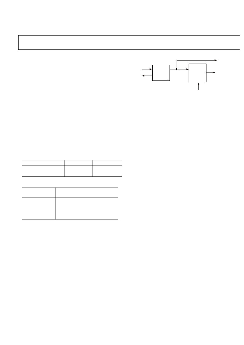
Figure 5
shows core to CLKIN ratios of 3:1, 8:1, and 16:1 with
external oscillator or crystal. Note that more ratios are possible
and can be set through software using the power management
control register (PMCTL). For more information, see the
ADSP-2126x SHARC DSP Core Manual
.
Use the exact timing information given. Do not attempt to
derive parameters from the addition or subtraction of others.
While addition or subtraction would yield meaningful results
for an individual device, the values given in this data sheet
reflect statistical variations and worst cases. Consequently, it is
not meaningful to add parameters to derive longer times.
See
Figure 30 on Page 37
under Test Conditions for voltage
reference levels.
Switching characteristics specify how the processor changes its
signals. Circuitry external to the processor must be designed for
compatibility with these signal characteristics. Switching char-
acteristics describe what the processor will do in a given
circumstance. Use switching characteristics to ensure that any
timing requirement of a device connected to the processor (such
as memory) is satisfied.
Timing requirements apply to signals that are controlled by cir-
cuitry external to the processor, such as the data input for a read
operation. Timing requirements guarantee that the processor
operates correctly with other devices.
Table 8. ADSP-21266 CLKOUT and CCLK Clock
Generation Operation
Timing Requirements
CLKIN
CCLK
Description
Input Clock
Core Clock
Calculation
1/t
CK
1/t
CCLK
Table 9. Clock Periods
Timing
Requirements
t
CK
t
CCLK
t
SCLK
t
SPICLK
Description
1
1
where:
SR = serial port-to-core clock ratio (wide range, determined by SPORT
CLKDIV)
SPIR = SPI-to-core clock ratio (wide range, determined by SPIBAUD
register)
DAI_Px = serial port clock
SPICLK = SPI clock
CLKIN Clock Period
(Processor) Core Clock Period
Serial Port Clock Period = (t
CCLK
) × SR
SPI Clock Period = (t
CCLK
) × SPIR
Figure 5. Core Clock and System Clock Relationship to CLKIN
CLKIN
CCLK
(CORE CLOCK)
PLLICLK
XTAL
XTAL
OSC
PLL
3:1, 8:1,
16:1
CLKOUT
CLK-CFG [1:0]
相關(guān)PDF資料 |
PDF描述 |
|---|---|
| ADSP-21266SKBC-2B | SHARC Embedded Processor |
| ADSP-21266SKBCZ-2B | SHARC Embedded Processor |
| ADSP-21266SKBCZ-2C | SHARC Embedded Processor |
| ADSP-21266SKBCZ-2D | SHARC Embedded Processor |
| ADSP-21266SKSTZ-1B | SHARC Embedded Processor |
相關(guān)代理商/技術(shù)參數(shù) |
參數(shù)描述 |
|---|---|
| ADSP-21266_07 | 制造商:AD 制造商全稱(chēng):Analog Devices 功能描述:Embedded Processor |
| ADSP-21266KSTZ-1C | 制造商:Analog Devices 功能描述:- Trays |
| ADSP-21266KSTZ-2C | 制造商:Analog Devices 功能描述:- Trays |
| ADSP-21266SKBC-2B | 制造商:Analog Devices 功能描述:DSP FLOATING PT 32BIT 200MHZ 200MIPS 136CSPBGA - Trays |
| ADSP-21266SKBCZ-2B | 制造商:Analog Devices 功能描述: |
發(fā)布緊急采購(gòu),3分鐘左右您將得到回復(fù)。