- 您現(xiàn)在的位置:買賣IC網(wǎng) > PDF目錄362152 > ADSP-2115BS-66 (ANALOG DEVICES INC) ADSP-2100 Family DSP Microcomputers PDF資料下載
參數(shù)資料
| 型號: | ADSP-2115BS-66 |
| 廠商: | ANALOG DEVICES INC |
| 元件分類: | 數(shù)字信號處理 |
| 英文描述: | ADSP-2100 Family DSP Microcomputers |
| 中文描述: | 24-BIT, 16.67 MHz, OTHER DSP, PQFP80 |
| 封裝: | METRIC, PLASTIC, QFP-80 |
| 文件頁數(shù): | 7/64頁 |
| 文件大小: | 666K |
| 代理商: | ADSP-2115BS-66 |
第1頁第2頁第3頁第4頁第5頁第6頁當前第7頁第8頁第9頁第10頁第11頁第12頁第13頁第14頁第15頁第16頁第17頁第18頁第19頁第20頁第21頁第22頁第23頁第24頁第25頁第26頁第27頁第28頁第29頁第30頁第31頁第32頁第33頁第34頁第35頁第36頁第37頁第38頁第39頁第40頁第41頁第42頁第43頁第44頁第45頁第46頁第47頁第48頁第49頁第50頁第51頁第52頁第53頁第54頁第55頁第56頁第57頁第58頁第59頁第60頁第61頁第62頁第63頁第64頁
ADSP-21xx
REV. B
–7–
T he interrupt force and clear register, IFC, is a write-only
register that contains a force bit and a clear bit for each inter-
rupt (except for level-sensitive interrupts and the ADSP-2111
HIP interrupts—these cannot be forced or cleared in software).
When responding to an interrupt, the AST AT , MST AT , and
IMASK status registers are pushed onto the status stack and
the PC counter is loaded with the appropriate vector address.
T he status stack is seven levels deep (nine levels deep on the
ADSP-2111) to allow interrupt nesting. T he stack is automati-
cally popped when a return from the interrupt instruction is
executed.
Pin Definitions
T able IV (on next page) shows pin definitions for the ADSP-
21xx processors. Any inputs not used must be tied to V
DD
.
T able III. Interrupt Vector Addresses & Priority
ADSP-2105
Interrupt
Source
Interrupt
Vector Address
RESET
Startup
IRQ2
SPORT 1 T ransmit
or
IRQ1
SPORT 1 Receive
or
IRQ0
T imer
0x0000
0x0004
(High Priority)
0x0010
0x0014
0x0018
(Low Priority)
ADSP-2101/2103/2115/216x
Interrupt
Source
Interrupt
Vector Address
RESET
Startup
IRQ2
SPORT 0 T ransmit
SPORT 0 Receive
SPORT 1 T ransmit
or
IRQ1
SPORT 1 Receive
or
IRQ0
T imer
0x0000
0x0004
(High Priority)
0x0008
0x000C
0x0010
0x0014
0x0018
(Low Priority)
ADSP-2111
Interrupt
Source
Interrupt
Vector Address
RESET
Startup
IRQ2
HIP Write from Host
HIP Read to Host
SPORT 0 T ransmit
SPORT 0 Receive
SPORT 1 T ransmit
or
IRQ1
SPORT 1 Receive
or
IRQ0
T imer
0x0000
0x0004
(High Priority)
0x0008
0x000C
0x0010
0x0014
0x0018
0x001C
0x0020
(Low Priority)
SY ST E M INT E RFACE
Figure 3 shows a typical system for the ADSP-2101, ADSP-
2115, or ADSP-2103, with two serial I/O devices, a boot
EPROM, and optional external program and data memory. A
total of 15K words of data memory and 16K words of program
memory is addressable for the ADSP-2101 and ADSP-2103. A
total of 14.5K words of data memory and 15K words of
program memory is addressable for the ADSP-2115.
Figure 4 shows a system diagram for the ADSP-2105, with one
serial I/O device, a boot EPROM, and optional external
program and data memory. A total of 14.5K words of data
memory and 15K words of program memory is addressable for
the ADSP-2105.
Figure 5 shows a system diagram for the ADSP-2111, with two
serial I/O devices, a host processor, a boot EPROM, and
optional external program and data memory. A total of 15K
words of data memory and 16K words of program memory is
addressable.
Programmable wait-state generation allows the processors to
easily interface to slow external memories.
T he ADSP-2101, ADSP-2103, ADSP-2115, and ADSP-2111
processors also provide either: one external interrupt (
IRQ2
)
and two serial ports (SPORT 0, SPORT 1),
or
three external
interrupts (
IRQ2
,
IRQ1
,
IRQ0
) and one serial port (SPORT 0).
T he ADSP-2105 provides either: one external interrupt (
IRQ2
)
and one serial port (SPORT 1),
or
three external interrupts
(
IRQ2
,
IRQ1
,
IRQ0
) with no serial port.
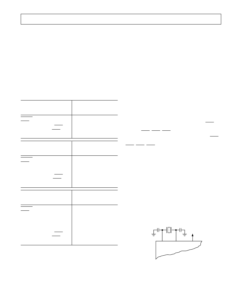
Clock Signals
T he ADSP-21xx processors’ CLK IN input may be driven by a
crystal or by a T T L-compatible external clock signal. T he
CLK IN input may not be halted or changed in frequency during
operation, nor operated below the specified low frequency limit.
If an external clock is used, it should be a T T L-compatible
signal running at the instruction rate. T he signal should be
connected to the processor’s CLK IN input; in this case, the
X T AL input must be left unconnected.
Because the ADSP-21xx processors include an on-chip oscilla-
tor circuit, an external crystal may also be used. T he crystal
should be connected across the CLK IN and X T AL pins, with
two capacitors connected as shown in Figure 2. A parallel-
resonant, fundamental frequency, microprocessor-grade crystal
should be used.
Figure 2. External Crystal Connections
CLKIN
CLKOUT
XTAL
ADSP-21xx
相關PDF資料 |
PDF描述 |
|---|---|
| ADSP-2115BS-80 | ADSP-2100 Family DSP Microcomputers |
| ADSP-2115BST-80 | ADSP-2100 Family DSP Microcomputers |
| ADSP-2101KS-100 | CAP 470PF 50V 5% NPO(C0G) SMD-0603 TR-7-PA |
| ADSP-2103KP-40 | ADSP-2100 Family DSP Microcomputers |
| ADSP-2105KP-55 | ADSP-2100 Family DSP Microcomputers |
相關代理商/技術參數(shù) |
參數(shù)描述 |
|---|---|
| ADSP-2115BS-80 | 制造商:Rochester Electronics LLC 功能描述:20MHZ MICROCOMPUTER IC - Bulk 制造商:Analog Devices 功能描述: |
| ADSP-2115BST-55 | 制造商:未知廠家 制造商全稱:未知廠家 功能描述:16-Bit Digital Signal Processor |
| ADSP-2115BST-66 | 制造商:AD 制造商全稱:Analog Devices 功能描述:ADSP-2100 Family DSP Microcomputers |
| ADSP-2115BST-80 | 制造商:AD 制造商全稱:Analog Devices 功能描述:ADSP-2100 Family DSP Microcomputers |
| ADSP-2115KP-100 | 制造商:Analog Devices 功能描述:DSP Fixed-Point 16-Bit 25MHz 25MIPS 68-Pin PLCC 制造商:Rochester Electronics LLC 功能描述:- Bulk |
發(fā)布緊急采購,3分鐘左右您將得到回復。