- 您現(xiàn)在的位置:買賣IC網(wǎng) > PDF目錄362145 > ADS7816 CMOS Quad 2-Input NOR Gate 14-SO -55 to 125 PDF資料下載
參數(shù)資料
| 型號: | ADS7816 |
| 英文描述: | CMOS Quad 2-Input NOR Gate 14-SO -55 to 125 |
| 中文描述: | 12位高速微功耗采樣模擬到數(shù)字轉(zhuǎn)換器 |
| 文件頁數(shù): | 10/13頁 |
| 文件大小: | 226K |
| 代理商: | ADS7816 |
10
ADS7816
D
OUT
1.4V
Test Point
3k
100pF
C
LOAD
t
r
D
OUT
V
OH
V
OL
t
f
t
dDO
t
hDO
D
OUT
DCLOCK
V
OH
V
OL
V
IL
D
OUT
Test Point
t
dis
Waveform 2, t
en
t
dis
Waveform 1
100pF
C
LOAD
3k
t
dis
CS/SHDN
D
OUT
Waveform 1
(1)
D
OUT
Waveform 2
(2)
90%
10%
V
IH
1
B11
2
t
en
CS/SHDN
DCLOCK
V
OL
D
OUT
V
CC
Load Circuit for t
dDO
, t
r
, and t
f
Voltage Waveforms for D
OUT
Rise and Fall TImes t
r
, and t
f
Voltage Waveforms for D
OUT
Delay Times, t
dDO
Load Circuit for t
dis
and t
den
Voltage Waveforms for t
en
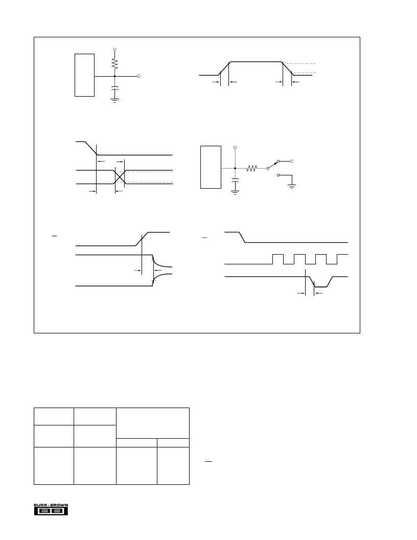
FIGURE 2. Timing Diagrams and Test Circuits for the Parameters in Table I.
Voltage Waveforms for t
dis
DESCRIPTION
ANALOG VALUE
Full Scale Range
V
REF
Least Significant
Bit (LSB)
V
REF
/4096
Full Scale
V
REF
–1 LSB
1111 1111 1111
FFF
Midscale
V
REF
/2
1000 0000 0000
800
Midscale – 1 LSB
V
REF
/2 – 1 LSB
0V
0111 1111 1111
7FF
Zero
0000 0000 0000
000
Table II. Ideal Input Voltages and Output Codes.
DIGITAL OUTPUT:
STRAIGHT BINARY
BINARY CODE
HEX CODE
NOTES: (1) Waveform 1 is for an output with internal conditions such that
the output is HIGH unless disabled by the output control. (2) Waveform 2
is for an output with internal conditions such that the output is LOW unless
disabled by the output control.
DATA FORMAT
The output data from the ADS7816 is in Straight Binary
format as shown in Table II. This table represents the ideal
output code for the given input voltage and does not include
the effects of offset, gain error, or noise.
POWER DISSIPATION
The architecture of the converter, the semiconductor fabrica-
tion process, and a careful design allow the ADS7816 to
convert at up to a 200kHz rate while requiring very little
power. Still, for the absolute lowest power dissipation, there
are several things to keep in mind.
The power dissipation of the ADS7816 scales directly with
conversion rate. The first step to achieving the lowest power
dissipation is to find the lowest conversion rate that will
satisfy the requirements of the system.
In addition, the ADS7816 is in power down mode under two
conditions: when the conversion is complete and whenever
CS is HIGH (see Figure 1). Ideally, each conversion should
occur as quickly as possible, preferably, at a 3.2MHz clock
rate. This way, the converter spends the longest possible
time in the power down mode. This is very important as the
相關PDF資料 |
PDF描述 |
|---|---|
| ADS7816B | 12-Bit High Speed Micro Power Sampling ANALOG-TO-DIGITAL CONVERTER |
| ADS7816C | 12-Bit High Speed Micro Power Sampling ANALOG-TO-DIGITAL CONVERTER |
| ADS7816UC | 12-Bit High Speed Micro Power Sampling ANALOG-TO-DIGITAL CONVERTER(226.72 k) |
| ADS7816EB | 12-Bit High Speed Micro Power Sampling ANALOG-TO-DIGITAL CONVERTER(226.72 k) |
| ADS7816EC | 3-Channel LED Ballaster with PWM; Package: MSOP; No of Pins: 10; Temperature Range: -40°C to +125°C |
相關代理商/技術參數(shù) |
參數(shù)描述 |
|---|---|
| ADS7816B | 制造商:BB 制造商全稱:BB 功能描述:12-Bit High Speed Micro Power Sampling ANALOG-TO-DIGITAL CONVERTER |
| ADS7816C | 制造商:Texas Instruments 功能描述: |
| ADS7816E | 制造商:Texas Instruments 功能描述: |
| ADS7816E/250 | 功能描述:模數(shù)轉(zhuǎn)換器 - ADC 12-Bit High Speed MicroPower Sampling RoHS:否 制造商:Texas Instruments 通道數(shù)量:2 結構:Sigma-Delta 轉(zhuǎn)換速率:125 SPs to 8 KSPs 分辨率:24 bit 輸入類型:Differential 信噪比:107 dB 接口類型:SPI 工作電源電壓:1.7 V to 3.6 V, 2.7 V to 5.25 V 最大工作溫度:+ 85 C 安裝風格:SMD/SMT 封裝 / 箱體:VQFN-32 |
| ADS7816E/250G4 | 功能描述:模數(shù)轉(zhuǎn)換器 - ADC 12-Bit High Speed MicroPower Sampling RoHS:否 制造商:Texas Instruments 通道數(shù)量:2 結構:Sigma-Delta 轉(zhuǎn)換速率:125 SPs to 8 KSPs 分辨率:24 bit 輸入類型:Differential 信噪比:107 dB 接口類型:SPI 工作電源電壓:1.7 V to 3.6 V, 2.7 V to 5.25 V 最大工作溫度:+ 85 C 安裝風格:SMD/SMT 封裝 / 箱體:VQFN-32 |
發(fā)布緊急采購,3分鐘左右您將得到回復。