- 您現(xiàn)在的位置:買賣IC網(wǎng) > PDF目錄165354 > ADS1251 (Texas Instruments, Inc.) "ResolutionPlus 24-Bit PDF資料下載
參數(shù)資料
| 型號(hào): | ADS1251 |
| 廠商: | Texas Instruments, Inc. |
| 英文描述: | "ResolutionPlus 24-Bit |
| 中文描述: | ResolutionPlus 24 位 20kHz 低功耗模數(shù)轉(zhuǎn)換器 |
| 文件頁(yè)數(shù): | 7/17頁(yè) |
| 文件大小: | 323K |
| 代理商: | ADS1251 |
第1頁(yè)第2頁(yè)第3頁(yè)第4頁(yè)第5頁(yè)第6頁(yè)當(dāng)前第7頁(yè)第8頁(yè)第9頁(yè)第10頁(yè)第11頁(yè)第12頁(yè)第13頁(yè)第14頁(yè)第15頁(yè)第16頁(yè)第17頁(yè)
ADS1251
15
SBAS184A
www.ti.com
analog input is at 4.096V, then the differential voltage mag-
nitude is 4.096V. This is the case regardless of which input
is at 0V and which is at 4.096V. The digital-output result,
however, is quite different. The analog-input differential volt-
age is given by the following equation:
+VIN – (–VIN)
A positive digital output is produced whenever the analog-
input differential voltage is positive, whereas a negative
digital output is produced whenever the differential is nega-
tive. For example, a positive full-scale output is produced
when the converter is configured with a 4.096V reference,
and the analog-input differential is 4.096V. The negative full-
scale output is produced when the differential voltage is –
4.096V. In each case, the actual input voltages must remain
within the –0.3V to +VDD range.
Actual Analog-Input Voltage—the voltage at any one ana-
log input relative to GND.
Full-Scale Range (FSR)—as with most A/D converters, the
full-scale range of the ADS1251 is defined as the input which
produces the positive full-scale digital output minus the input
which produces the negative full-scale digital output. For
example, when the converter is configured with a 4.096V
reference, the differential full-scale range is:
[4.096V (positive full-scale) – (–4.096V) (negative full-scale)] = 8.192V
Least Significant Bit (LSB) Weight—this is the theoretical
amount of voltage that the differential voltage at the analog
input would have to change in order to observe a change in
the output data of one least significant bit. It is computed as
follows:
LSB Weight
Full ScaleRange
V
N
REF
N
=
=
21
2
21
–
–
where N is the number of bits in the digital output.
Conversion Cycle—as used here, a conversion cycle refers
to the time period between DOUT/DRDY pulses.
Effective Resolution (ER)—of the ADS1251, in a particular
configuration, can be expressed in two different units:
bits rms (referenced to output) and
Vrms (referenced to
input). Computed directly from the converter’s output data,
each is a statistical calculation based on a given number of
results. Noise occurs randomly; the rms value represents a
statistical measure, which is one standard deviation. The ER
in bits can be computed as follows:
ER in bits rms =
20 log
2
V
Vrms noise
REF
602
.
The 2 VREF figure in each calculation represents the full-
scale range of the ADS1251. This means that both units are
absolute expressions of resolution—the performance in dif-
ferent configurations can be directly compared, regardless of
the units.
fMOD—frequency of the modulator and the frequency the
input is sampled.
f
CLK Frequency
MOD =
6
fDATA—Data output rate.
f
CLK Frequency
DATA
MOD
==
64
384
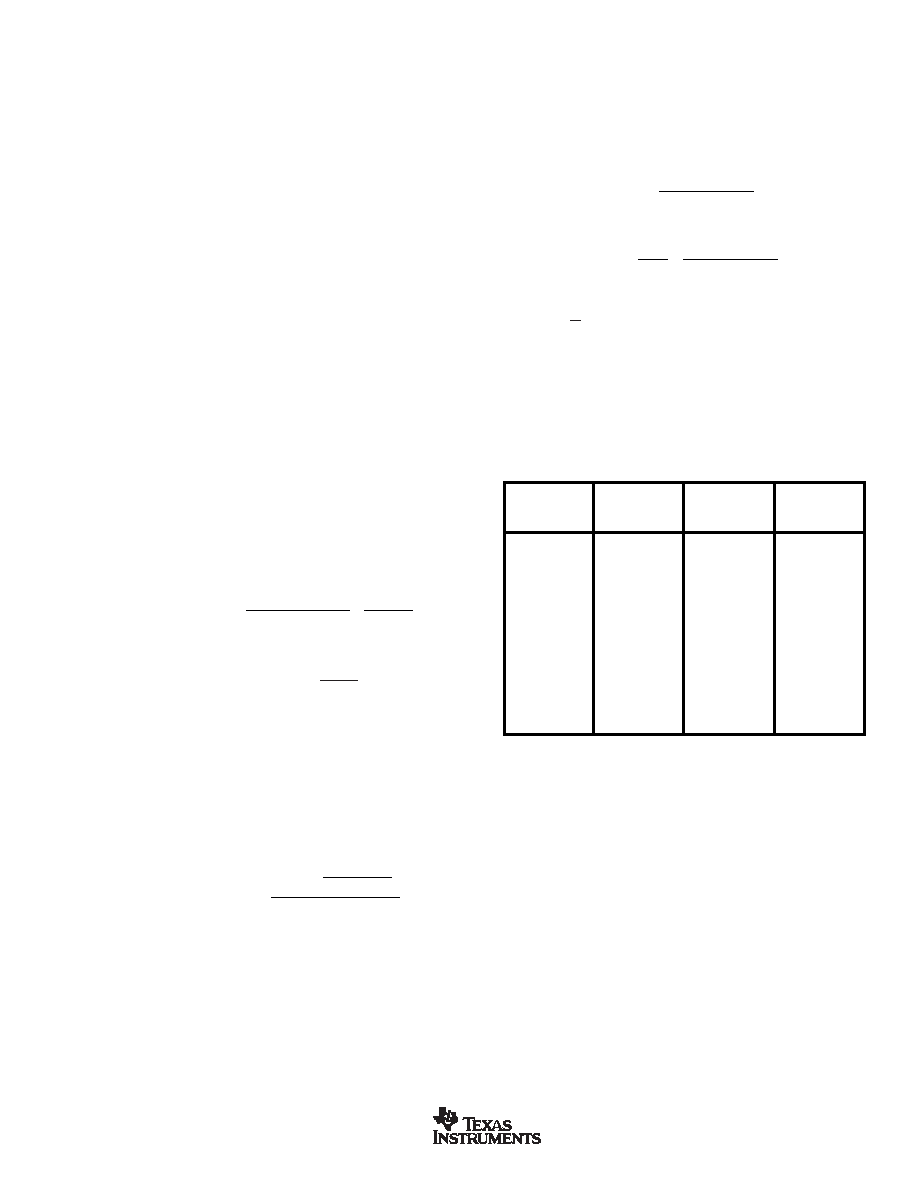
Noise Reduction—for random noise, the ER can be im-
proved with averaging. The result is the reduction in noise by
the factor
√N(yùn), where N is the number of averages, as shown
in Table IV. This can be used to achieve true 24-bit perfor-
mance at a lower data rate. To achieve 24 bits of resolution,
more than 24 bits must be accumulated. A 36-bit accumulator
is required to achieve an ER of 24 bits. The following uses
VREF = 4.096V, with the ADS1251 outputting data at 20kHz, a
4096 point average will take 204.8ms. The benefits of averag-
ing will be degraded if the input signal drifts during that 200ms.
N
NOISE
ER
(Number
REDUCTION
IN
of Averages)
FACTOR
Vrms
BITS rms
11
16
V
19.26
2
1.414
11.3
V
19.75
42
8
V
20.26
8
2.82
5.66
V
20.76
16
4
V
21.26
32
5.66
2.83
V
21.76
64
8
2
V
22.26
128
11.3
1.41
V
22.76
256
16
1
V
23.26
512
22.6
0.71
V
23.76
1024
32
0.5
V
24.26
2048
45.25
0.35
V
24.76
4096
64
0.25
V
25.26
TABLE IV. Averaging for Noise Reduction.
相關(guān)PDF資料 |
PDF描述 |
|---|---|
| ADS5102IPFBR | 1.8-V ANALOG SUPPLY, 10-BIT, 65/40 MSPS ANALOG-TO-DIGITAL CONVERTERS WITH INTERNAL REFERENCE |
| ADS5103 | "10 Bit |
| ADS5103CPFB | 1.8-V ANALOG SUPPLY, 10-BIT, 65/40 MSPS ANALOG-TO-DIGITAL CONVERTERS WITH INTERNAL REFERENCE |
| ADS5103CPFBR | 1.8-V ANALOG SUPPLY, 10-BIT, 65/40 MSPS ANALOG-TO-DIGITAL CONVERTERS WITH INTERNAL REFERENCE |
| ADS5103EVM | 1.8-V ANALOG SUPPLY, 10-BIT, 65/40 MSPS ANALOG-TO-DIGITAL CONVERTERS WITH INTERNAL REFERENCE |
相關(guān)代理商/技術(shù)參數(shù) |
參數(shù)描述 |
|---|---|
| ADS1251EVM | 功能描述:數(shù)據(jù)轉(zhuǎn)換 IC 開(kāi)發(fā)工具 ADS1251 ADC Eval Mod RoHS:否 制造商:Texas Instruments 產(chǎn)品:Demonstration Kits 類型:ADC 工具用于評(píng)估:ADS130E08 接口類型:SPI 工作電源電壓:- 6 V to + 6 V |
| ADS1251U | 功能描述:模數(shù)轉(zhuǎn)換器 - ADC ResolutionPlus 24Bit 20kHz Lo-Power RoHS:否 制造商:Texas Instruments 通道數(shù)量:2 結(jié)構(gòu):Sigma-Delta 轉(zhuǎn)換速率:125 SPs to 8 KSPs 分辨率:24 bit 輸入類型:Differential 信噪比:107 dB 接口類型:SPI 工作電源電壓:1.7 V to 3.6 V, 2.7 V to 5.25 V 最大工作溫度:+ 85 C 安裝風(fēng)格:SMD/SMT 封裝 / 箱體:VQFN-32 |
| ADS1251U | 制造商:Texas Instruments 功能描述:IC 24BIT ADC SMD 1251 SOIC8 |
| ADS1251U | 制造商:Texas Instruments 功能描述:IC ADC 24BIT 20KSPS SOIC-8 |
| ADS1251U/2K5 | 功能描述:模數(shù)轉(zhuǎn)換器 - ADC ResolutionPlus 24Bit 20kHz Lo-Power RoHS:否 制造商:Texas Instruments 通道數(shù)量:2 結(jié)構(gòu):Sigma-Delta 轉(zhuǎn)換速率:125 SPs to 8 KSPs 分辨率:24 bit 輸入類型:Differential 信噪比:107 dB 接口類型:SPI 工作電源電壓:1.7 V to 3.6 V, 2.7 V to 5.25 V 最大工作溫度:+ 85 C 安裝風(fēng)格:SMD/SMT 封裝 / 箱體:VQFN-32 |
發(fā)布緊急采購(gòu),3分鐘左右您將得到回復(fù)。