- 您現(xiàn)在的位置:買賣IC網(wǎng) > PDF目錄374022 > ADP3604AR (ANALOG DEVICES INC) Secondary Over-Voltage Protection for 2-4 cell in series Li-Ion/Poly (4.45V) 8-SM8 -40 to 110 PDF資料下載
參數(shù)資料
| 型號: | ADP3604AR |
| 廠商: | ANALOG DEVICES INC |
| 元件分類: | 穩(wěn)壓器 |
| 英文描述: | Secondary Over-Voltage Protection for 2-4 cell in series Li-Ion/Poly (4.45V) 8-SM8 -40 to 110 |
| 中文描述: | SWITCHED CAPACITOR REGULATOR, 140 kHz SWITCHING FREQ-MAX, PDSO8 |
| 封裝: | SOIC-8 |
| 文件頁數(shù): | 4/8頁 |
| 文件大?。?/td> | 143K |
| 代理商: | ADP3604AR |
ADP3604
REV. 0
–4–
APPLICAT ION INFORMAT ION
T he ADP3604 uses a charge pump to generate a negative out-
put voltage from a positive input supply. T o understand the
operation of the ADP3604, a review of a basic switch capacitor
building block is helpful.
f
R
L
V1
V2
C1
C2
A
B
Figure 11. Basic Switch Capacitor Circuit
In Figure 11, when the switch is in the A position, capacitor C1
will be charged to voltage V1. T he total charge on C1 will be
q1 = C1V1.
T he switch then moves to the B position, discharging C1 to
voltage V2. After this discharge time, the charge on C1 is q2 =
C1V2. T he amount of charge transferred from the source, V1,
to the output, V2 is:
q
=
q
1 –
q
2 =
C
1(
V
1 –
V
2)
If the switch is cycled
f
times per second, the charge transfer
per unit time (i.e., current) is:
I
=
f
q
=
fC
1(
V
1 –
V
2)
T o obtain an equivalent resistance for the switched-capacitor
network we can rewrite this equation in terms of voltage and
impedance equivalence:
I
= (
V
1 –
V
2)/(1/
fC
1) = (
V
1 –
V
2)/
R
EQUIV
where
R
EQUIV
is defined as :
R
EQUIV
= 1/
fC
1
Figure 11 equivalent circuit now can be drawn as shown in
Figure 12.
R
L
V1
V2
C2
R
EQUIV
R
EQUIV =
1
fC1
Figure 12. Basic Switch Capacitor Equivalent Circuit
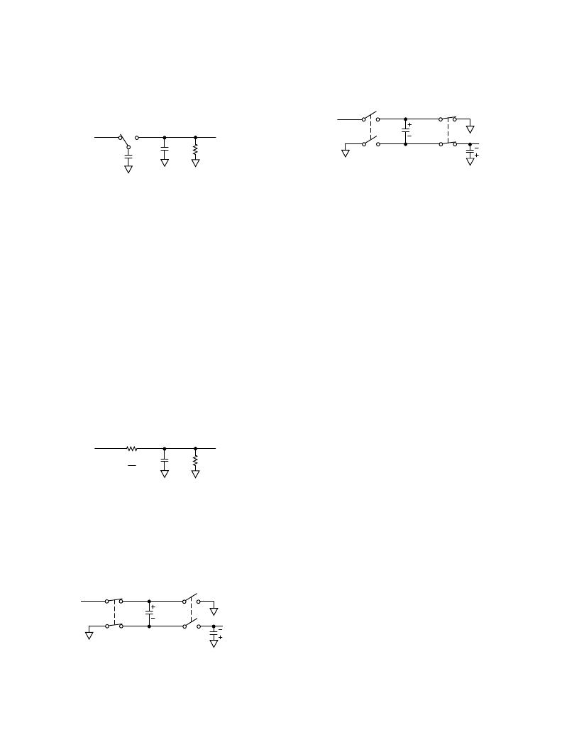
T HE ORY OF OPE RAT ION
A switched capacitor principle is used in the ADP3604 to gener-
ate a negative voltage from a positive input voltage. An on-board
oscillator generates two phase clocks to control a switching net-
work which transfers charge between the storage capacitors.
T he basic principle behind the voltage inversion scheme is illus-
trated in Figures 13 and 14.
V
IN
S2
C
P
S1
V
OUT
S3
S4
C
OUT
Figure 13. Switch Configuration Charging the Pump
Capacitor
During phase one, S1 and S2 are ON charging the pump ca-
pacitor to the input voltage. Before the next phase begins, S1
and S2
are turned OFF as well as S3 and S4 to prevent any
overlap. S3 and S4
are turned ON during the second phase (see
Figure 14) and charge stored in the pump capacitor is trans-
ferred to the output capacitor.
V
IN
S2
C
P
S1
V
OUT
S3
S4
C
OUT
Figure 14. Switch Configuration Charging the Output
Capacitor
During the second phase, the positive terminal of the pump
capacitor is connected to ground and the negative terminal is
connected to the output resulting in a voltage inversion at the
output terminal. Output regulation is done by adjusting the ON
resistance of the S3 through the feedback control loop.
T he ADP3604 alternately charges C
P
to the input voltage when
C
P
is switched in parallel with the input supply, and then trans-
fers charge to C
OUT
when C
P
is switched in parallel with C
OUT
.
Switching occurs at 120 kHz rate. During the time that C
P
is
charging, the peak current is approximately 2 times the output
current. During the time that C
P
is delivering charge to C
OUT
,
the supply current drops down to about 2 mA. An input supply
bypass capacitor will supply part of the peak input current drawn
by the ADP3604, and average out the current drawn from the
supply. A minimum input supply bypass capacitor of 1
μ
f,
preferably a low ESR capacitor such as tantalum or multilayer
ceramic chip capacitor, is recommended. A large capacitor may
be desirable in some cases, for example when the input supply is
connected to the ADP3604 through long leads, or when the
pulse current drawn by the device might effect other circuitry
through supply coupling.
T he output capacitor, C
OUT
, is alternately charged to the C
P
voltage when C
P
is switched in parallel with C
OUT
. T he ESR of
the C
OUT
introduces steps in the V
OUT
waveform whenever the
charge pump charges C
OUT
. T his tends to increase V
OUT
ripple.
Ceramic or tantalum capacitors are recommended for C
OUT
if
minimum ripple is desired. T he ADP3604 can operate with a
range of capacitors from 1
μ
f to 100
μ
f and larger without any
stability problems. However, all tested parameters are obtained
using 10
μ
f multilayer ceramic capacitors.
In most applications, IR drops due to printed circuit board
traces do not present a problem. In this case, V
SENSE
is tied to
the output at a convenient pcb location not far from the V
OUT
.
However, if a reduction in IR drops or improvement in load
regulation is desired, the sense line can be used to monitor the
output voltage at the load. T o avoid excessive noise pickup, the
V
SENSE
line should be as short as possible and away from any
noisy line.
While the exact values of the C
IN
and C
OUT
are not critical, good
quality, low ESR capacitors such as solid tantalum and multi-
layer ceramic capacitors are recommended to minimize voltage
losses at high currents. For a given load current, factors affecting
the output voltage performance in Figure 15 are:
Pump (C2) and the output (C3) capacitance
ESR of the C2 and C3
相關(guān)PDF資料 |
PDF描述 |
|---|---|
| ADP3604* | Dual/Quad Rail-to-Rail Output, Picoamp Input Precision Op Amps; Package: SO; No of Pins: 8; Temperature Range: -40°C to +85°C |
| ADP3605ARU-3 | 120 mA Switched Capacitor Voltage Inverter with Regulated Output |
| ADP3605AR-3 | 120 mA Switched Capacitor Voltage Inverter with Regulated Output |
| ADP3605AR | Secondary Over-Voltage Protection for 2-4 cell in series Li-Ion/Poly (4.45V) 8-SM8 -40 to 110 |
| ADP3605 | 120 mA Switched Capacitor Voltage Inverter with Regulated Output(穩(wěn)壓輸出的開關(guān)電容電壓反相器) |
相關(guān)代理商/技術(shù)參數(shù) |
參數(shù)描述 |
|---|---|
| ADP3604AR-REEL | 制造商:Analog Devices 功能描述: |
| ADP3605 | 制造商:AD 制造商全稱:Analog Devices 功能描述:120 mA Switched Capacitor Voltage Inverter with Regulated Output |
| ADP36050001RUR | 制造商:Analog Devices 功能描述: |
| ADP3605AR | 制造商:Analog Devices 功能描述:Charge Pump INV -3V to -6V 120mA 8-Pin SOIC N 制造商:Analog Devices 功能描述:IC VOLTAGE REGULATOR |
| ADP3605AR-3 | 制造商:Analog Devices 功能描述:Charge Pump INV -3V 120mA 8-Pin SOIC N |
發(fā)布緊急采購,3分鐘左右您將得到回復(fù)。