- 您現(xiàn)在的位置:買(mǎi)賣IC網(wǎng) > PDF目錄374022 > ADP3412JR (ANALOG DEVICES INC) Secondary Over-Voltage Protection for 2-4 cell in series Li-Ion/Poly (4.35V) 8-SM8 -40 to 110 PDF資料下載
參數(shù)資料
| 型號(hào): | ADP3412JR |
| 廠商: | ANALOG DEVICES INC |
| 元件分類: | MOSFETs |
| 英文描述: | Secondary Over-Voltage Protection for 2-4 cell in series Li-Ion/Poly (4.35V) 8-SM8 -40 to 110 |
| 中文描述: | BUF OR INV BASED MOSFET DRIVER, PDSO8 |
| 封裝: | SOIC-8 |
| 文件頁(yè)數(shù): | 3/8頁(yè) |
| 文件大小: | 135K |
| 代理商: | ADP3412JR |
ADP3412
–3–
REV. 0
PIN FUNCTION DESCRIPTIONS
Pin
Mnemonic
Function
1
BST
Floating Bootstrap Supply for the Upper MOSFET. A capacitor connected between BST and SW pins
holds this bootstrapped voltage for the high-side MOSFET as it is switched. The capacitor should be
chosen between 100 nF and 1 F.
TTL-level Input Signal, which has primary control of the drive outputs.
Low-High Transition Delay. A capacitor from this pin to ground programs the propagation delay from
turn-off of the lower FET to turn-on of the upper FET. The formula for the low-high transition delay
is DLY = C
DLY
×
(1 ns/pF) + 20 ns. The rise time for turn-on of the upper FET is not included in the formula.
Input Supply. This pin should be bypassed to PGND with ~1
μ
F ceramic capacitor.
Synchronous Rectifier Drive. Output drive for the lower (synchronous rectifier) MOSFET.
Power Ground. Should be closely connected to the source of the lower MOSFET.
This pin is connected to the buck-switching node, close to the upper MOSFET
’
s source. It is the floating
return for the upper MOSFET drive signal. It is also used to monitor the switched voltage to prevent turn-
on of the lower MOSFET until the voltage is below ~1 V. Thus, according to operating conditions, the
high-low transition delay is determined at this pin.
Buck Drive. Output drive for the upper (buck) MOSFET.
2
3
IN
DLY
4
5
6
7
VCC
DRVL
PGND
SW
8
DRVH
ORDERING GUIDE
Model
Temperature Range
0
°
C to 70
°
C
Package Description
Package Option
ADP3412JR
8-Lead Standard Small Outline Package (SOIC)
R-8
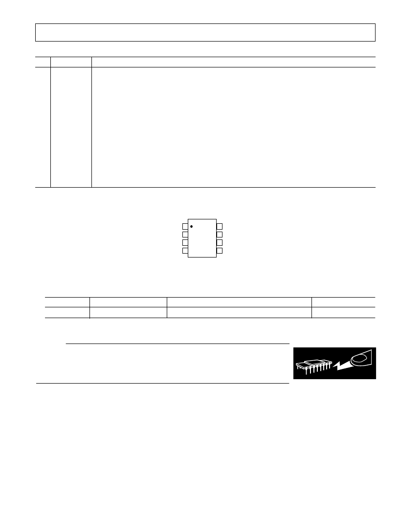
PIN CONFIGURATION
1
2
3
4
8
7
6
5
TOP VIEW
(Not to Scale)
ADP3412
BST
IN
DLY
VCC
DRVH
SW
PGND
DRVL
CAUTION
ESD (electrostatic discharge) sensitive device. Electrostatic charges as high as 4000 V readily
accumulate on the human body and test equipment and can discharge without detection. Although
the ADP3412 features proprietary ESD protection circuitry, permanent damage may occur on
devices subjected to high-energy electrostatic discharges. Therefore, proper ESD precautions are
recommended to avoid performance degradation or loss of functionality.
WARNING!
ESD SENSITIVE DEVICE
相關(guān)PDF資料 |
PDF描述 |
|---|---|
| ADP3413 | Secondary Over-Voltage Protection for 2-4 cell in series Li-Ion/Poly (4.35V) 8-SM8 -40 to 110 |
| ADP3413JR | Secondary Over-Voltage Protection for 2-4 cell in series Li-Ion/Poly (4.35V) 8-SM8 -40 to 110 |
| ADP3414 | Secondary Over-Voltage Protection for 2-4 cell in series Li-Ion/Poly (4.35V) 8-SM8 -40 to 110 |
| ADP3414JR | Secondary Over-Voltage Protection for 2-4 cell in series Li-Ion/Poly (4.35V) 8-SM8 -40 to 110 |
| ADP3416 | Dual Bootstrapped MOSFET Driver |
相關(guān)代理商/技術(shù)參數(shù) |
參數(shù)描述 |
|---|---|
| ADP3412JR-REEL | 制造商:Rochester Electronics LLC 功能描述:HIGH CURRENT DUAL MOSFET DRIVER - Tape and Reel |
| ADP3412JR-REEL7 | 制造商:Rochester Electronics LLC 功能描述:- Tape and Reel |
| ADP3412JRZ-REEL | 制造商:Analog Devices 功能描述: |
| ADP3413 | 制造商:AD 制造商全稱:Analog Devices 功能描述:Dual Bootstrapped MOSFET Driver with Output Disable |
| ADP3413JR | 制造商:Rochester Electronics LLC 功能描述:HIGH CURRENT DUAL FET DRIVER W/DISABLE - Bulk |
發(fā)布緊急采購(gòu),3分鐘左右您將得到回復(fù)。