- 您現(xiàn)在的位置:買賣IC網(wǎng) > PDF目錄374021 > ADP3310 (Analog Devices, Inc.) Precision Regulator Controllers(精密穩(wěn)壓控制器) PDF資料下載
參數(shù)資料
| 型號: | ADP3310 |
| 廠商: | Analog Devices, Inc. |
| 英文描述: | Precision Regulator Controllers(精密穩(wěn)壓控制器) |
| 中文描述: | 精密穩(wěn)壓器控制器(精密穩(wěn)壓控制器) |
| 文件頁數(shù): | 7/8頁 |
| 文件大小: | 197K |
| 代理商: | ADP3310 |
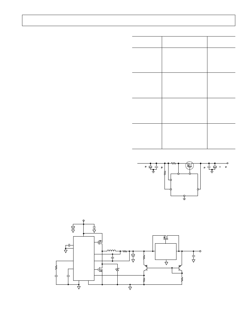
ADP3310
–7–
REV. 0
ADP3310-3.3
GND
IN
OUT
GATE
MI
IRF7404
+
OSCON
220μF
C1
1μF
V
IN
= 5V TO 15V
C2
10nF
IRF7204
L*
68μH
N-CH
IRF7403
C3
1nF
D1
10BQ040
C4
R
SENSE
**
R1
30.1k
1%
2N3906
Q1
R2
124k
1%
R
C
1k
C
C
22nF
C
T
470pF
R3
274k
2N3906
Q2
C5
10μF
3.3V/1A
V
IN
INT V
CC
ADP1148
P-DRIVE
I
TH
CT
SENSE
+
SENSE
–
N-DRIVE
FB
S-GND P-GND
SD
C
IN
OSCON
220μF
*
* COILTRONICS CTX-68-4
** KRL SL-1-C1-ORO5OL
Figure 15. High Current Post Regulator with SOIC PMOS
Current Limit Threshold Voltage = 0.05 V
Safety Factor = 1.5
I
O
= Output Current
R
S
is not needed in circuits that do not require current limiting.
In that case, the I
S
pin must be tied to the input pin.
The simplest and cheapest sense resistor for high current applica-
tions, (i.e., Figure 1) is a PCB trace. The temperature depen-
dence of the copper trace and the thickness tolerances of the
trace must be taken into account in the design. The resistivity of
copper has a positive temperature coefficient of +0.39%/
°
C.
Copper’s Tempco in conjunction with the proportional-to-
absolute temperature (PTAT) current limit voltage can provide
an accurate current limit. Table III provides the resistance value
for PCB copper traces. Alternately, an appropriate sense resistor
such as surface mount sense resistors available from KRL can be
used.
PCB-Layout Issues
For optimum voltage regulation, place the load as close as
possible to the device’s V
OUT
and GND pins. It is recommended
to use dedicated PCB traces to connect the MOSFET’s drain to
the positive terminal and GND to the negative terminal of the
load to avoid voltage drops along the high current carrying PCB
traces.
Application Circuits
Typical 3 A LDO Circuit
The ADP3310 and a power MOSFET can be used to power the
new generation of CPUs and microprocessors from the standard
+5 V supply at a very low cost (Figure 14). This circuit provides
low dropout, fast switching and high switching load current
from 0 A to 3 A. Due to the high switching load current, capaci-
tors with high ripple current carrying capability, such as OSCON
or special tantalum capacitors from Sprague (593D), are recom-
mended for the output.
Table III. Printed Circuit Copper Resistance
Conductor
Thickness
Conductor Width
In
Resistance
m
/In
1/2 oz/ft
2
(18
μ
m)
0.025
0.050
0.100
0.200
0.500
39.3
19.7
9.83
4.91
1.97
1 oz/ft
2
(35
μ
m)
0.025
0.050
0.200
0.500
19.7
9.83
2.46
0.98
2 oz/ft
2
(70
μ
m)
0.025
0.050
0.100
0.200
0.500
9.83
4.91
2.46
1.23
0.49
3 oz/ft
2
(106
μ
m)
0.025
0.050
0.100
0.200
0.500
6.5
3.25
1.63
0.81
0.325
M1
NDP6020P
10 F
4.5V TO 5.5V
10 F
IS
GND
EN
V
IN
V
OUT
ADP3310-3.3
+
R2
0.011
GATE
1k
220 F
OSCON
+
3 220 F
OSCON
3.3V
Figure 14. Typical 3 A Low Dropout Regulator Circuit
50mV/div
2V/div
5
μ
s/div
相關PDF資料 |
PDF描述 |
|---|---|
| ADP3330ART-25 | Cap-Free, NMOS, 150mA Low Dropout Regulator with Reverse Current Protection |
| ADP3330ART-5 | OMAP Compatible Fuel Gauge for 1 & 2 Cell Li-Ion 8-TSSOP -20 to 70 |
| ADP3330ART-2.5 | THREE-TERMINAL POSITIVE FIXED VOLTAGE REGULATORS |
| ADP3330ART-2.75 | THREE-TERMINAL POSITIVE FIXED VOLTAGE REGULATORS |
| ADP3330ART-2.85 | THREE-TERMINAL POSITIVE FIXED VOLTAGE REGULATORS |
相關代理商/技術參數(shù) |
參數(shù)描述 |
|---|---|
| ADP3310AR-2.8 | 制造商:Rochester Electronics LLC 功能描述:- Bulk 制造商:Analog Devices 功能描述: |
| ADP3310AR-28 | 制造商:AD 制造商全稱:Analog Devices 功能描述:Precision Voltage Regulator Controller |
| ADP3310AR-3 | 制造商:Rochester Electronics LLC 功能描述:- Bulk |
| ADP3310AR-3.3 | 制造商:Rochester Electronics LLC 功能描述:LOW DROPOUT-REGULATOR CONTROLLER - Bulk |
| ADP3310AR-3.3-REEL | 制造商:Rochester Electronics LLC 功能描述:LOW DROPOUT-REGULATOR CONTROLLER - Tape and Reel |
發(fā)布緊急采購,3分鐘左右您將得到回復。