- 您現(xiàn)在的位置:買賣IC網(wǎng) > PDF目錄374021 > ADP3308ART-285 (Analog Devices, Inc.) anyCAP⑩ 50 mA Low Dropout Linear Regulator PDF資料下載
參數(shù)資料
| 型號(hào): | ADP3308ART-285 |
| 廠商: | Analog Devices, Inc. |
| 英文描述: | anyCAP⑩ 50 mA Low Dropout Linear Regulator |
| 中文描述: | anyCAP⑩50毫安低壓差線性穩(wěn)壓器 |
| 文件頁(yè)數(shù): | 3/8頁(yè) |
| 文件大小: | 115K |
| 代理商: | ADP3308ART-285 |
ADP3308
–3–
REV. A
ABSOLUTE MAXIMUM RATINGS*
Input Supply Voltage . . . . . . . . . . . . . . . . . . . –0.3 V to +16 V
Shutdown Input Voltage . . . . . . . . . . . . . . . . –0.3 V to +16 V
Power Dissipation . . . . . . . . . . . . . . . . . . . .Internally Limited
Operating Ambient Temperature Range . . . –55
°
C to +125
°
C
Operating Junction Temperature Range . . . –55
°
C to +125
°
C
θ
JA
. . . . . . . . . . . . . . . . . . . . . . . . . . . . . . . . . . . . 165
°
C/W
θ
JC
. . . . . . . . . . . . . . . . . . . . . . . . . . . . . . . . . . . . . 92
°
C/W
Storage Temperature Range . . . . . . . . . . . . –65
°
C to +150
°
C
Lead Temperature Range (Soldering 10 sec) . . . . . . . .+300
°
C
Vapor Phase (60 sec) . . . . . . . . . . . . . . . . . . . . . . . .+215
°
C
Infrared (15 sec) . . . . . . . . . . . . . . . . . . . . . . . . . . . .+220
°
C
*This is a stress rating only; operation beyond these limits can cause the device to
be permanently damaged.
ORDERING GUIDE
Voltage
Output
Package
Option*
Marking
Code
Model
ADP3308ART-2.7
ADP3308ART-2.85
ADP3308ART-2.9
ADP3308ART-3
ADP3308ART-3.3
ADP3308ART-3.6
2.7 V
2.85 V
2.9 V
3.0 V
3.3 V
3.6 V
SOT-23
SOT-23
SOT-23
SOT-23
SOT-23
SOT-23
DAC
DJC
DKC
DCC
DEC
DFC
*SOT = Surface Mount.
Contact the factory for the availability of other output voltage options.
Other Member of anyCAP Family
1
Model
Output Current
Package Option
2
ADP3309
100 mA
SOT-23-5 Lead
NOTES
1
See individual data sheet for detailed ordering information.
2
SOT = Surface Mount.
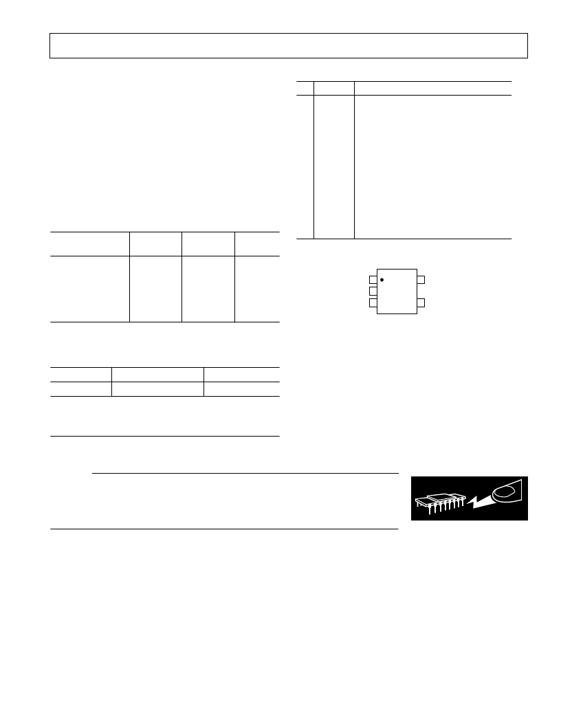
PIN FUNCTION DESCRIPTIONS
Pin Name
Function
1
2
3
IN
GND
SD
Regulator Input.
Ground Pin.
Active Low Shutdown Pin. Connect to
ground to disable the regulator output.
When shutdown is not used, this pin
should be connected to the input pin.
Open Collector. Output that goes low
to indicate the output is about to go out
of regulation or no connect.
Output of the Regulator, fixed 2.7, 2.85,
2.9, 3.0, 3.3, or 3.6 volts output voltage.
Bypass to ground with a 0.47
μ
F or larger
capacitor.
4
ERR
/NC
5
OUT
PIN CONFIGURATION
1
2
3
4
5
TOP VIEW
(Not to Scale)
IN
GND
OUT
ADP3308
SD
ERR
/NC
NC = NO CONNECT
CAUTION
ESD (electrostatic discharge) sensitive device. Electrostatic charges as high as 4000 V readily
accumulate on the human body and test equipment and can discharge without detection.
Although the ADP3308 features proprietary ESD protection circuitry, permanent damage may
occur on devices subjected to high energy electrostatic discharges. Therefore, proper ESD
precautions are recommended to avoid performance degradation or loss of functionality.
WARNING!
ESD SENSITIVE DEVICE
相關(guān)PDF資料 |
PDF描述 |
|---|---|
| ADP3308ART-29 | Circular Connector; No. of Contacts:3; Series:; Body Material:Aluminum Alloy; Connecting Termination:Solder; Connector Shell Size:20; Circular Contact Gender:Pin; Circular Shell Style:Cable Receptacle; Insert Arrangement:20-19 RoHS Compliant: No |
| ADP3308ART-3 | AB 9C 1#12 8#16 SKT RECP |
| ADP3308ART-33 | anyCAP⑩ 50 mA Low Dropout Linear Regulator |
| ADP3308ART-36 | anyCAP⑩ 50 mA Low Dropout Linear Regulator |
| ADP3309ART-27 | anyCAP⑩ 100 mA Low Dropout Linear Regulator |
相關(guān)代理商/技術(shù)參數(shù) |
參數(shù)描述 |
|---|---|
| ADP3308ART-29 | 制造商:AD 制造商全稱:Analog Devices 功能描述:anyCAP⑩ 50 mA Low Dropout Linear Regulator |
| ADP3308ART-3 | 制造商:AD 制造商全稱:Analog Devices 功能描述:anyCAP⑩ 50 mA Low Dropout Linear Regulator |
| ADP3308ART-3.3 | 制造商:未知廠家 制造商全稱:未知廠家 功能描述:Positive Fixed Voltage Regulator |
| ADP3308ART-3.3-RL | 制造商:Rochester Electronics LLC 功能描述:- Tape and Reel 制造商:Analog Devices 功能描述: |
| ADP3308ART-3.3-RL7 | 制造商:Rochester Electronics LLC 功能描述:- Bulk |
發(fā)布緊急采購(gòu),3分鐘左右您將得到回復(fù)。