- 您現(xiàn)在的位置:買賣IC網(wǎng) > PDF目錄374016 > ADM9240ARU (ANALOG DEVICES INC) Low Cost Microprocessor System Hardware Monitor PDF資料下載
參數(shù)資料
| 型號: | ADM9240ARU |
| 廠商: | ANALOG DEVICES INC |
| 元件分類: | 電源管理 |
| 英文描述: | Low Cost Microprocessor System Hardware Monitor |
| 中文描述: | 9-CHANNEL POWER SUPPLY SUPPORT CKT, PDSO24 |
| 封裝: | TSSOP-24 |
| 文件頁數(shù): | 8/22頁 |
| 文件大?。?/td> | 280K |
| 代理商: | ADM9240ARU |
ADM9240
–8–
REV. 0
When reading data from a register there are two possibilities:
1. If the ADM9240’s Address Pointer Register value is un-
known or not the desired value, it is first necessary to set it to
the correct value before data can be read from the desired
data register. T his is done by performing a write to the
ADM9240 as before, but only the data byte containing the
register address is sent, as data is not to be written to the
register. T his is shown in Figure 2b.
A read operation is then performed consisting of the serial
bus address, R/
W
bit set to 1, followed by the data byte read
from the data register. T his is shown in Figure 2c.
2. If the Address Pointer Register is known to be already at the
desired address, data can be read from the corresponding
data register without first writing to the Address Pointer
Register, so Figure 2b can be omitted.
Notes:
1. Although it is possible to read a data byte from a data register
without first writing to the Address Pointer Register, if the
Address Pointer Register is already at the correct value, it is
not possible to write data to a register without writing to the
Address Pointer Register, because the first data byte of a
write is always written to the Address Pointer Register.
2. In Figures 2a to 2c, the serial bus address is shown as the
default value 01011(A1)(A0), where A1 and A0 are
hardwired to either Logic 0 or Logic 1.
ANALOG INPUT S
T he ADM9240 has six analog inputs. Four of these are dedi-
cated to monitoring the following power supply voltages: +12 V,
+5 V, +3.3 V, +2.5 V.
T hese inputs are multiplexed into the on-chip, successive ap-
proximation, analog-to-digital converter. T his has a resolution
of ten bits, but only eight bits are used for the voltage measure-
ment and limit comparison. T he basic input range of the ADC
is 0 V to 2.5 V, and the power supply inputs are scaled by on-
chip attenuators such that the ADC produces an output of 3/4
×
full scale or 192 decimal, when the input voltage is at its nomi-
nal value. T he use of on-chip scaling guarantees accuracy and
removes the need for precision external resistors.
R/
W
0
SCL
SDA
1
0
1
1
A1
A0
D7
D6
D5
D4
D3
D2
D1
D0
ACK. BY
ADM9240
STOP BY
MASTER
START BY
MASTER
FRAME 1
SERIAL BUS ADDRESS BYTE
FRAME 2
ADDRESS POINTER REGISTER BYTE
1
9
1
ACK. BY
ADM9240
9
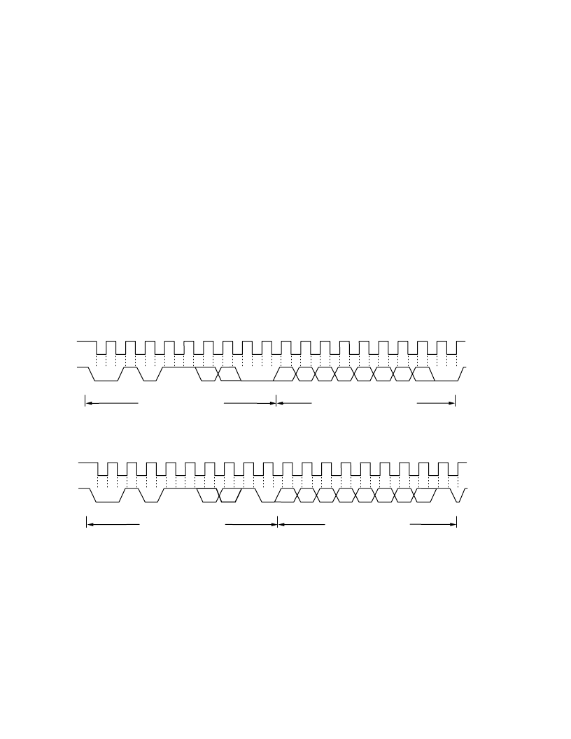
Figure 2b. Writing to the Address Pointer Register only
R/
W
0
SCL
SDA
1
0
1
1
A1
A0
D7
D6
D5
D4
D3
D2
D1
D0
NO ACK.
BY MASTER
STOP BY
MASTER
START BY
MASTER
FRAME 1
SERIAL BUS ADDRESS BYTE
FRAME 2
DATA BYTE FROM ADM9240
1
9
1
ACK. BY
ADM9240
9
Figure 2c. Reading Data from a Previously Selected Register
相關(guān)PDF資料 |
PDF描述 |
|---|---|
| ADM9261 | Triple- Power Supply Monitor(3路電源監(jiān)視器) |
| ADM9264ARN-REEL | Quad Power Supply Monitor for Desktop PCs |
| ADM9264ARN-REEL7 | Quad Power Supply Monitor for Desktop PCs |
| ADM9264 | Quad Power Supply Monitor for Desktop PCs |
| ADM9264ARN | Quad Power Supply Monitor for Desktop PCs |
相關(guān)代理商/技術(shù)參數(shù) |
參數(shù)描述 |
|---|---|
| ADM9240ARU-REEL | 制造商:AD 制造商全稱:Analog Devices 功能描述:Low Cost Microprocessor System Hardware Monitor |
| ADM9240ARU-REEL7 | 制造商:Analog Devices 功能描述: |
| ADM9264 | 制造商:AD 制造商全稱:Analog Devices 功能描述:Quad Power Supply Monitor for Desktop PCs |
| ADM9264ARN | 制造商:Analog Devices 功能描述:Volt Supervisor Monitor 2.8V/3.3V/5V/12V 16-Pin SOIC N 制造商:Rochester Electronics LLC 功能描述:MULTI-SUPPLY HARDWARE MON - Bulk |
| ADM9264ARN-REEL | 制造商:Rochester Electronics LLC 功能描述:- Tape and Reel |
發(fā)布緊急采購,3分鐘左右您將得到回復(fù)。