- 您現(xiàn)在的位置:買賣IC網(wǎng) > PDF目錄374011 > ADM805M (Analog Devices, Inc.) Microprocessor Supervisory Circuits PDF資料下載
參數(shù)資料
| 型號: | ADM805M |
| 廠商: | Analog Devices, Inc. |
| 英文描述: | Microprocessor Supervisory Circuits |
| 中文描述: | 微處理器監(jiān)控電路 |
| 文件頁數(shù): | 6/8頁 |
| 文件大?。?/td> | 327K |
| 代理商: | ADM805M |
ADM690A/ADM692A/ADM802L/M/ADM805L/M
–6–
REV. 0
Table I. Input and Output Status in Battery Backup Mode
Signal
Status
V
OUT
V
OUT
is connected to V
BATT
via an internal
PMOS switch.
Logic low.
Logic high (ADM805L, ADM805M). The open
circuit output voltage is equal to V
OUT
.
The power fail comparator is disabled
Logic low.
The watchdog timer is disabled
RESET
RESET
PFI
PFO
WDI
Power Fail Comparator
The power fail comparator is an independent comparator
that may be used to monitor the input power supply. The
comparator’s inverting input is internally connected to a 1.25
V reference voltage. The noninverting input is available at the
PFI input. This input may be used to monitor the input power
supply via a resistive divider network. When the voltage on the
PFI input drops below 1.25 V, the comparator output (
PFO
)
goes low indicating a power failure. For early warning of power
failure the comparator may be used to monitor the preregulator
input simply by choosing an appropriate resistive divider
network. The
PFO
output can be used to interrupt the
processor so that a shutdown procedure is implemented before
the power is lost.
1.25V
POWER FAIL
OUTPUT
(PFO)
POWER
FAIL
INPUT
INPUT
POWER
R1
R2
Figure 9. Power Fail Comparator
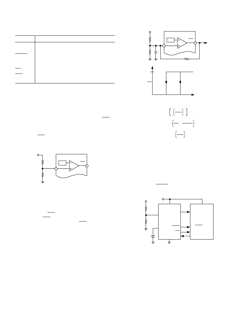
Adding Hysteresis to the Power Fail Comparator
For increased noise immunity, hysteresis may be added to the
power fail comparator. Since the comparator circuit is non-
inverting, hysteresis can be added simply by connecting a
resistor between the
PFO
output and the PFI input as shown in
Figure 10. When
PFO
is low, resistor R3 sinks current from the
summing junction at the PFI pin. When
PFO
is high, resistor
R3 sources current into the PFI summing junction. This results
in differing trip levels for the comparator. Further noise
immunity may be achieved by connecting a capacitor between
PFI and GND.
1.25V
(PFO)
INPUT
POWER
R1
R2
PFI
R3
TO
μP NMI
5V
PFO
0V
0V
V
L
V
H
V
IN
V
H
= 1.25 1+R2
×
R3
V
L
= 125+R1
1.25 –
CC
–1.25
R2
R3
V
MID
= 1.25
R1+R2
R2
Figure 10. Adding Hysteresis to the Power Fail
Comparator
TYPICAL APPLICATIONS
Figure 11 shows a typical power monitoring, battery backup
application. V
OUT
powers the CMOS RAM. Under normal
operating conditions with V
CC
present, V
OUT
is internally
connected to V
CC
. If a power failure occurs, V
CC
will decay and
V
OUT
will be switched to V
BATT
thereby maintaining power for
the CMOS RAM. A
RESET
pulse is also generated when V
CC
falls below the reset threshold.
CMOS RAM
POWER
μP RESET
μP NMI
I/O LINE
μP SYSTEM
V
CC
μP POWER
V
OUT
RESET
PFO
WDI
GND
V
BATT
PFI
UNREGULATED
DC
R1
R2
+5V
BATTERY
+
Figure 11. Typical Application Circuit
The watchdog timer input (WDI) monitors an I/O line from the
μ
P system. This line must be toggled once every 1.6 seconds to
verify correct software execution. Failure to toggle the line
indicates that the
μ
P system is not correctly executing its
program and may be tied up in an endless loop. If this happens,
a reset pulse is generated to initialize the processor.
相關(guān)PDF資料 |
PDF描述 |
|---|---|
| ADM805MAN | Microprocessor Supervisory Circuits |
| ADM805MARN | Microprocessor Supervisory Circuits |
| ADM690AAN | Microprocessor Supervisory Circuits |
| ADM690AARM | Microprocessor Supervisory Circuits |
| ADM690AARN | Microprocessor Supervisory Circuits |
相關(guān)代理商/技術(shù)參數(shù) |
參數(shù)描述 |
|---|---|
| ADM805MAN | 制造商:Analog Devices 功能描述:Processor Supervisor 4.4V 4.4V 8-Pin PDIP 制造商:Analog Devices 功能描述:PROCESSOR SUPERVISOR 4.4V 100UA 8PDIP - Rail/Tube |
| ADM805MARN | 制造商:AD 制造商全稱:Analog Devices 功能描述:Microprocessor Supervisory Circuits |
| ADM809 | 制造商:AD 制造商全稱:Analog Devices 功能描述:Microprocessor Supervisory Circuit in 3-Pin SOT-23 |
| ADM809-5AKSZ | 制造商:Analog Devices 功能描述: |
| ADM809-5L | 制造商:AD 制造商全稱:Analog Devices 功能描述:Microprocessor Supervisory Circuit |
發(fā)布緊急采購,3分鐘左右您將得到回復(fù)。