REV.
ADM222/ADM232A/ADM242
鈥�3鈥�
ABSOLUTE MAXIMUM RATINGS
*
(TA = 25
掳C unless otherwise noted)
VCC . . . . . . . . . . . . . . . . . . . . . . . . . . . . . . . . . . . . . . . . . . 6 V
V+ . . . . . . . . . . . . . . . . . . . . . . . . . . . (VCC 鈥� 0.3 V) to +13 V
V鈥� . . . . . . . . . . . . . . . . . . . . . . . . . . . . . . . . . +0.3 V to 鈥�13 V
Input Voltages
TIN
. . . . . . . . . . . . . . . . . . . . . . . . 鈥�0.3 V to (VCC + 0.3 V)
RIN
. . . . . . . . . . . . . . . . . . . . . . . . . . . . . . . . . . . . .
卤30 V
Output Voltages
TOUT . . . . . . . . . . . . . . . . . . . (V+, +0.3 V) to (V鈥�, 鈥�0.3 V)
ROUT . . . . . . . . . . . . . . . . . . . . . . . 鈥�0.3 V to (VCC + 0.3 V)
Short Circuit Duration
TOUT . . . . . . . . . . . . . . . . . . . . . . . . . . . . . . . . Continuous
Power Dissipation N-16 . . . . . . . . . . . . . . . . . . . . . . 400 mW
(Derate 7.5 mW/
掳C above 70掳C)
胃JA, Thermal Impedance . . . . . . . . . . . . . . . . . . . . 80掳C/W
Power Dissipation R-16N . . . . . . . . . . . . . . . . . . . . . 400 mW
(Derate 7 mW/
掳C above 70掳C)
胃JA, Thermal Impedance . . . . . . . . . . . . . . . . . . . . 80掳C/W
Power Dissipation R-16W . . . . . . . . . . . . . . . . . . . . . 400 mW
(Derate 7 mW/
掳C above 70掳C)
胃JA, Thermal Impedance . . . . . . . . . . . . . . . . . . . . 80掳CW
Power Dissipation N-18 . . . . . . . . . . . . . . . . . . . . . . 400 mW
(Derate 7 mW/
掳C above 70掳C)
胃JA, Thermal Impedance . . . . . . . . . . . . . . . . . . . . 80掳C/W
Power Dissipation R-18W . . . . . . . . . . . . . . . . . . . . . 400 mW
(Derate 7 mW/
掳C above 70掳C)
胃JA, Thermal Impedance . . . . . . . . . . . . . . . . . . . . 80掳C/W
Operating Temperature Range
Industrial (A Version) . . . . . . . . . . . . . . .
鈥�40
掳C to +85掳C
Storage Temperature Range . . . . . . . . . . . . 鈥�65
掳C to +150掳C
Lead Temperature (Soldering, 10 sec) . . . . . . . . . . . . 300
掳C
Vapor Phase (60 sec) . . . . . . . . . . . . . . . . . . . . . . . . 215
掳C
Infrared (15 sec) . . . . . . . . . . . . . . . . . . . . . . . . . . . . . 220
掳C
*This is a stress rating only and functional operation of the device at these or any
other conditions above those indicated in the operation sections of this specifica-
tion is not implied. Exposure to absolute maximum rating conditions for extended
periods of time may affect reliability.
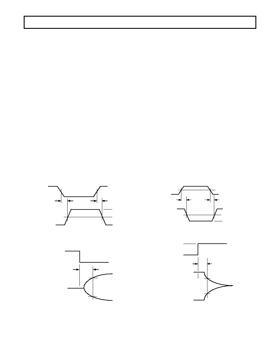
Test Circuits
V鈥�
V+
0V
VOUT
3V
VIN
tPHLT
tPLHT
Figure 1. Transmitter Propagation Delay Timing
0.8V
3V
3.5V
RECEIVER
OUTPUT
EN
INPUT
0V
tER
Figure 2. Receiver Enable Timing
tPHLR
tPLHR
GND
VCC
50%
VIN
VOUT
3V
0V
Figure 3. Receiver Propagation Delay Timing
VOH 鈥� 0.5V
RECEIVER
OUTPUT
EN
INPUT
VOL + 0.5V
VOH
VOL
0V
3V
tDR
Figure 4. Receiver Disable Timing
B
