- 您現(xiàn)在的位置:買賣IC網(wǎng) > PDF目錄57599 > ADL5371ACPZ-R7 (ANALOG DEVICES INC) 700 MHz - 1300 MHz RF/MICROWAVE QUADRAPHASE MODULATOR PDF資料下載
參數(shù)資料
| 型號(hào): | ADL5371ACPZ-R7 |
| 廠商: | ANALOG DEVICES INC |
| 元件分類: | 調(diào)制器/解調(diào)器 |
| 英文描述: | 700 MHz - 1300 MHz RF/MICROWAVE QUADRAPHASE MODULATOR |
| 封裝: | LEAD FREE, MO-220VGGD-2, LFCSP-24 |
| 文件頁(yè)數(shù): | 5/7頁(yè) |
| 文件大?。?/td> | 277K |
| 代理商: | ADL5371ACPZ-R7 |
Preliminary Technical Data
ADL5373 / ADL5374
Rev. PrJ | Page 5 of 7
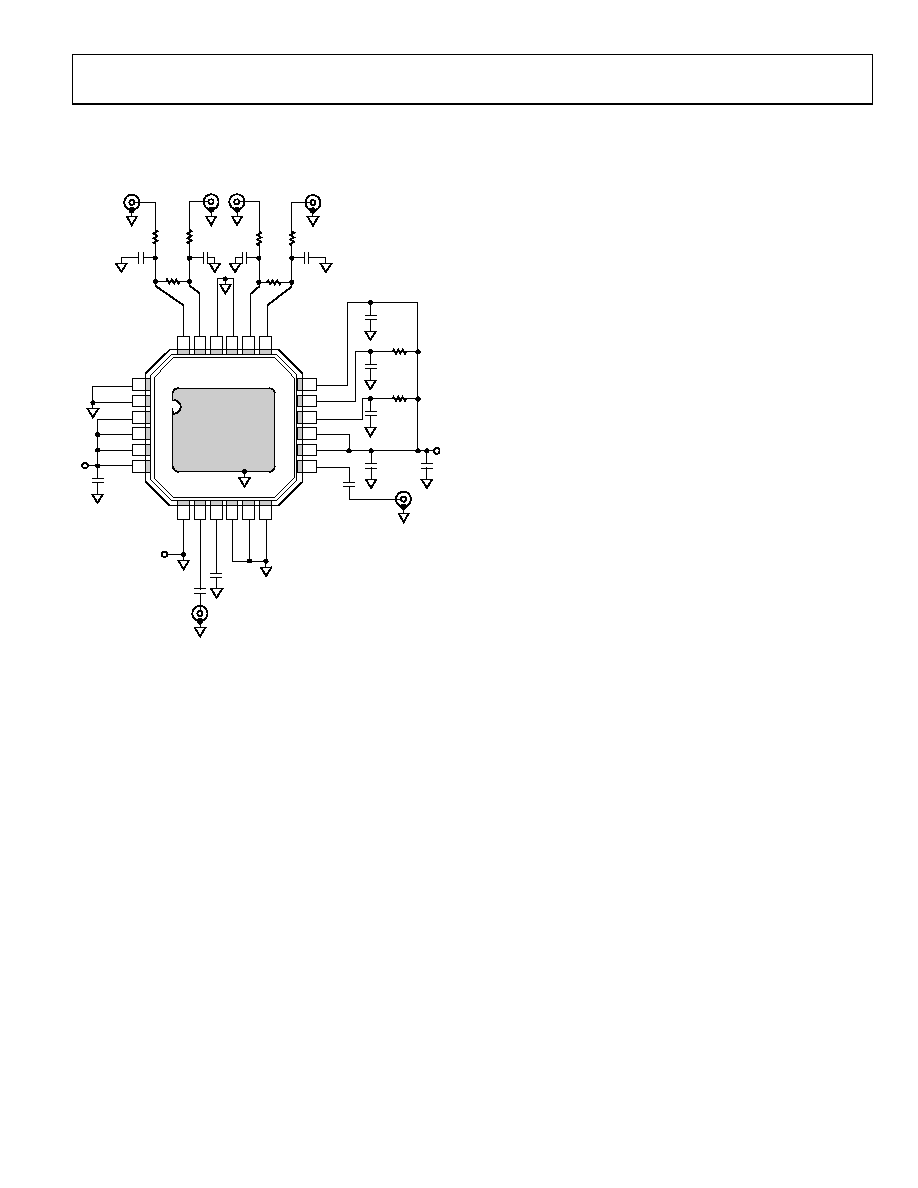
BASIC CONNECTIONS
Figure 3 shows the basic connections for the F-MOD.
VPS5
VPS3
VPS4
VPS2
VOUT
CO
M
2
LOI
N
LOI
P
CO
M
2
CO
M
3
CO
M
3
Q
BBP
CO
M
4
Q
BBN
CO
M
4
IB
B
N
IB
B
P
COM1
VPS1
COM1
VPS1
1
2
3
4
5
6
18
17
16
15
14
13
VOUT
C13
0.1F
C12
0.1F
CLON
100pF
C14
0.1F
C15
0.1F
C16
0.1F
24
23
22
21
20
19
7
8
9
10
11
12
COUT
100pF
L12
0
L11
0
VP
O
S
RFNQ
0
RFPQ
0
QBBP
QBBN
IBBN
IBBP
RFNI
0
RFPI
0
CFNQ
OPEN
CFPQ
OPEN
CFPI
OPEN
CFNI
OPEN
RTI
OPEN
RTQ
OPEN
EXPOSED PADDLE
CLOP
100pF
LO
GND
Z1
FMOD
VPO
S
Figure 3. Basic Connections for the F-MOD
Power Supply and Grounding
All the VPS pins must be connected to the same 5 V source.
Adjacent pins of the same name can be tied together and decoupled
with a 0.1 μF capacitor. These capacitors should be located as
close as possible to the device. The power supply can range
between 4.75 V and 5.25 V.
The COM1 pin, COM2 pin, and COM3 pin should be tied to
the same ground plane through low impedance paths. The exposed
paddle on the underside of the package should also be soldered
to a low thermal and electrical impedance ground plane. If the
ground plane spans multiple layers on the circuit board, they
should be stitched together with nine vias under the exposed
paddle. The Analog Devices AN-772 application note discusses
the thermal and electrical grounding of the LFCSP_VQ in
greater detail.
Baseband Inputs
The baseband inputs QBBP, QBBN, IBBP, and IBBN must be
driven from a differential source. The nominal drive level of
1.4 V p-p differential (700 mV p-p on each pin) should be
biased to a common-mode level of 500 mV dc.
The dc common-mode bias level for the baseband inputs may
range from 400 mV to 600 mV. This results in a reduction in
the usable input ac swing range. The nominal dc bias of 500 mV
allows for the largest ac swing, limited on the bottom end by the
F-MOD input range and on the top end by the output compliance
range on most digital-to-analog converters (DAC) from Analog
Devices.
LO Input
A single-ended LO signal should be applied to the LOIP pin
through an ac-coupling capacitor. The recommended LO drive
power is 0 dBm. The LO return pin, LOIN, should be ac-coupled
to ground through a low impedance path.
The nominal LO drive of 0 dBm can be increased to up to 7 dBm.
RF Output
The ground-referenced RF output is available at the VOUT pin
(Pin 13). This pin should be ac-coupled to the load.
相關(guān)PDF資料 |
PDF描述 |
|---|---|
| ADL5372ACPZ-R7 | 1500 MHz - 2500 MHz RF/MICROWAVE QUADRAPHASE MODULATOR |
| ADL5372ACPZ-WP | 1500 MHz - 2500 MHz RF/MICROWAVE QUADRAPHASE MODULATOR |
| ADP-0105-20-000-02 | 0 MHz - 18000 MHz RF/MICROWAVE FIXED ATTENUATOR |
| ADP-0107-01-000-02 | 0 MHz - 18000 MHz RF/MICROWAVE FIXED ATTENUATOR |
| ADP-0106-04-000-02 | 0 MHz - 18000 MHz RF/MICROWAVE FIXED ATTENUATOR |
相關(guān)代理商/技術(shù)參數(shù) |
參數(shù)描述 |
|---|---|
| ADL5371ACPZ-WP | 制造商:Analog Devices 功能描述:QUADRATURE MOD 700MHZ 24LFCSP EP - Waffle Pack |
| ADL5371-EVALZ | 制造商:Analog Devices 功能描述:EVAL BOARD - Bulk |
| ADL5372 | 制造商:AD 制造商全稱:Analog Devices 功能描述:400 MHz to 6 GHz Broadband Quadrature Modulator |
| ADL5372ACPZ-R2 | 制造商:Analog Devices 功能描述:1500 MHZ TO 2500 MHZ QUADRATURE MODULATOR - Tape and Reel |
| ADL5372ACPZ-R21 | 制造商:AD 制造商全稱:Analog Devices 功能描述:1500 MHz to 2500 MHz Quadrature Modulator |
發(fā)布緊急采購(gòu),3分鐘左右您將得到回復(fù)。