- 您現(xiàn)在的位置:買賣IC網(wǎng) > PDF目錄373978 > ADD8708WSTZ-REEL (ANALOG DEVICES INC) 18-Channel Gamma Buffer with Regulator PDF資料下載
參數(shù)資料
| 型號(hào): | ADD8708WSTZ-REEL |
| 廠商: | ANALOG DEVICES INC |
| 元件分類: | 運(yùn)動(dòng)控制電子 |
| 英文描述: | 18-Channel Gamma Buffer with Regulator |
| 中文描述: | 18 BUFFER AMPLIFIER, PQFP48 |
| 封裝: | LEAD FREE, MO-026-BBC, LQFP-48 |
| 文件頁數(shù): | 10/16頁 |
| 文件大?。?/td> | 454K |
| 代理商: | ADD8708WSTZ-REEL |
ADD8708
APPLICATION NOTES
The ADD8708 is a mask-programmable gamma reference
generator that allows source drivers to be optimized for the
different combinations of liquid crystals, glass sizes, etc. in
large LCD panels. It generates 18 gamma reference outputs
that can be mask-programmed in 0.2% increments using the
500 matched internal resistors (see Figure 20), so that every
point on the curve can be targeted within 0.1% of the desired
value.
Rev. 0 | Page 10 of 16
0
TAP POINT 4
TAP POINT 3
TAP POINT 2
TAP POINT 1
TAP POINT 500
TAP POINT 499
TAP POINT 498
TAP POINT 497
EACH R = 30
TYPICALLY
Figure 20. 500 Mask-Programmable Resistor String
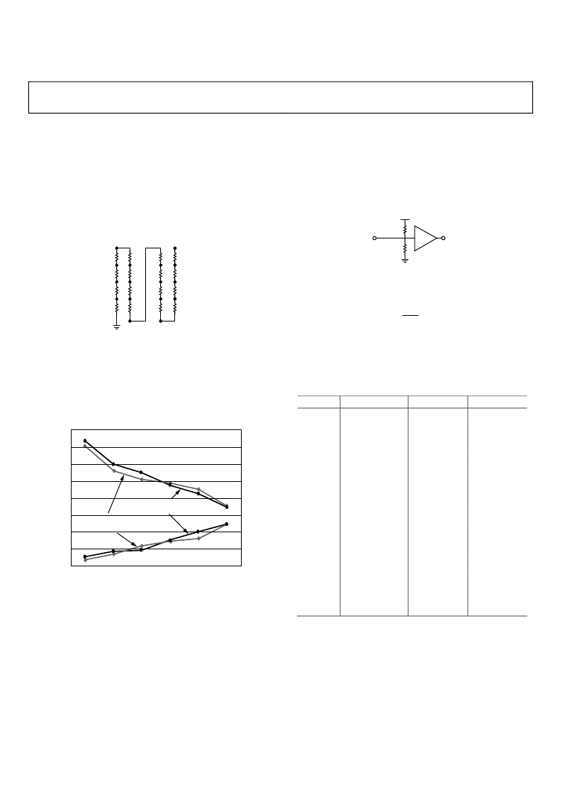
In a typical panel application, the selected source drivers have
an internal gamma curve that is not ideal for the specific panel
(see Figure 21). The ADD8708 allows the gamma curve in the
source drivers to be adjusted appropriately, and also ensures
that all the source drivers have the same gamma curve.
16
14
12
10
PANEL GAMMA CURVE
CORRECTED BY ADD8708
ORIGINAL GAMMA CURVE
IN SOURCE DRIVERS
8
6
4
2
0
0
GAMMA REFERENCE INPUT POINTS
G
Figure 21. Original and Corrected Gamma Curves
The matching and tracking accuracy of the internal resistors is
typically 0.1% with worst-case deviation from the desired curve
within 0.4% of the ideal gamma curve, over temperature.
The ADD8708 also includes a low-dropout linear regulator to
provide a stable reference level for the gamma curve for
optimum panel performance.
TAP POINT SELECTION
The ADD8708 uses a single resistor string consisting of 500
individual elements. The tap points are mask programmable
and completely independent of each other. See the Tap Point
and Regulator Voltage Request Form in this data sheet.
0
V
REG OUT
V
OUT
X
V
IN
X
500–TP
X
TP
X
Figure 22. Gamma Buffers Tap Point Circuit
Tap point voltages can be derived from the following equation:
TP
X
V
=
500
OUT
REG
X
OUT
V
×
where
TP
X
is the desired tap point for the X
th
channel.
Table 5. Typical Mask Implementation
1
V
DD
= 16 V, V
REG OUT
= 14.4 V, 0 ≤ X ≤ 500
Tap Point (X)
V
OUT
18
500
V
OUT
17
396
V
OUT
16
369
V
OUT
15
361
V
OUT
14
354
V
OUT
13
350
V
OUT
12
341
V
OUT
11
317
V
OUT
10
299
V
OUT
9
225
V
OUT
8
211
V
OUT
7
177
V
OUT
6
167
V
OUT
5
163
V
OUT
4
154
V
OUT
3
146
V
OUT
2
118
V
OUT
1
7
Voltage
14.400
11.405
10.627
10.397
10.195
10.080
9.821
9.130
8.611
6.480
6.077
5.098
4.810
4.694
4.435
4.205
3.398
0.202
Units
V
V
V
V
V
V
V
V
V
V
V
V
V
V
V
V
V
V
_______________________________
1
ADD8708 release samples do not have these typical values. The values on the
samples are nonmonotonic and can be provided upon request.
相關(guān)PDF資料 |
PDF描述 |
|---|---|
| ADD8709 | 18-Channel Gamma Buffer with Regulator |
| ADD8709ASTZ-REEL | 18-Channel Gamma Buffer with Regulator |
| ADD8709ASTZ-REEL7 | 18-Channel Gamma Buffer with Regulator |
| ADD8710 | 10 - CHANNEL GAMMA BUFFER WITH V-COM DRIVER |
| ADD8710ARUZ | 10 - CHANNEL GAMMA BUFFER WITH V-COM DRIVER |
相關(guān)代理商/技術(shù)參數(shù) |
參數(shù)描述 |
|---|---|
| ADD8709 | 制造商:AD 制造商全稱:Analog Devices 功能描述:18-Channel Gamma Buffer with Regulator |
| ADD8709ASTZ-REEL | 制造商:Rochester Electronics LLC 功能描述: 制造商:Analog Devices 功能描述: |
| ADD8709ASTZ-REEL7 | 制造商:Rochester Electronics LLC 功能描述: 制造商:Analog Devices 功能描述: |
| ADD8709WSTZ-REEL7 | 制造商:Rochester Electronics LLC 功能描述: 制造商:Analog Devices 功能描述: |
| ADD8710 | 制造商:AD 制造商全稱:Analog Devices 功能描述:10 - CHANNEL GAMMA BUFFER WITH V-COM DRIVER |
發(fā)布緊急采購(gòu),3分鐘左右您將得到回復(fù)。