- 您現(xiàn)在的位置:買賣IC網(wǎng) > PDF目錄373978 > ADD8708WCPZ-REEL7 (ANALOG DEVICES INC) 18-Channel Gamma Buffer with Regulator PDF資料下載
參數(shù)資料
| 型號(hào): | ADD8708WCPZ-REEL7 |
| 廠商: | ANALOG DEVICES INC |
| 元件分類: | 運(yùn)動(dòng)控制電子 |
| 英文描述: | 18-Channel Gamma Buffer with Regulator |
| 中文描述: | 18 BUFFER AMPLIFIER, QCC48 |
| 封裝: | LEAD FREE, MO-220-VKKD, LFCSP-48 |
| 文件頁(yè)數(shù): | 3/16頁(yè) |
| 文件大小: | 454K |
| 代理商: | ADD8708WCPZ-REEL7 |
第1頁(yè)第2頁(yè)當(dāng)前第3頁(yè)第4頁(yè)第5頁(yè)第6頁(yè)第7頁(yè)第8頁(yè)第9頁(yè)第10頁(yè)第11頁(yè)第12頁(yè)第13頁(yè)第14頁(yè)第15頁(yè)第16頁(yè)
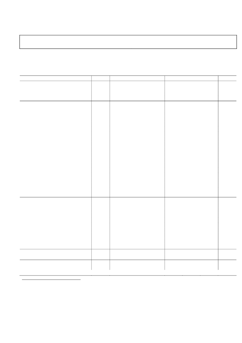
ADD8708
ELECTRICAL CHARACTERISTICS
V
DD
= 16 V, T
A
@ 25°C, unless otherwise noted.
Rev. 0 | Page 3 of 16
Table 1.
Parameter
GAMMA CURVE CHARACTERISTICS
Accuracy
Programming Resolution
Total Resistor String
BUFFER CHARACTERISTICS
OUTPUTS
Output Voltage Range (Ch18 to Ch10)
Output Voltage Range (Ch9 to Ch1)
Output vs. Load (Ch18, Ch17, Ch2, Ch1)
Output vs. Load (Ch16 to Ch3)
INPUTS
Offset Voltage
Offset Voltage Drift
Input Bias Current
Input Voltage Range (Ch18 to Ch10)
Input Voltage Range (Ch9 to Ch1)
DYNAMIC PERFORMANCE
Slew Rate
Bandwidth
Settling Time to 0.1%
Phase Margin
Power Supply Rejection Ratio
Symbol
R
ACC1
R
RES
R
TOTAL
V
OUT
V
OUT
V
OUT2
V
OUT2
V
OS
V
OS
/T
I
B
V
IN
V
IN
SR
BW
t
S
Ф
o
PSRR
Conditions
500 segments
I
L
= 100 μA
I
L
= 100 μA
I
L
= 20 mA
I
L
= 5 mA
40°C ≤ T
A
≤ +105°C
40°C ≤ T
A
≤ +105°C
R
L
= 10 k, C
L
= 200 pF
–3 dB, R
L
= 10 k, C
L
= 200 pF
1 V, R
L
= 10 k, C
L
= 200 pF
R
L
= 10 k, C
L
= 200 pF
V
DD
= 7 V to 17 V,
40°C ≤ T
A
≤ +105°C
No load; V
REG OUT
= 14.4V
I
L
= 100 μA
I
L
= 5 mA
V
IN
= 8.5 V to 16.5 V, V
OUT
= 8 V
I
O
= 100 μA to 10 mA
40°C ≤ T
A
≤ +105°C
40°C ≤ T
A
≤ +105°C
40°C ≤ T
A
≤ +105°C
No load;
40°C ≤ T
A
≤ +105°C
Min
1.4
0
1.4
0
4
68
Typ
0.1
0.2
15
15
5
5
20
0.5
6
4.5
1.1
55
90
Max
0.4
V
DD
V
DD
1.4
15
1.5
V
DD
V
DD
1.4
Unit
%
%
k
V
V
mV
mV
mV
μV/°C
μA
V
V
V/μs
MHz
μs
Degrees
dB
VOLTAGE REGULATOR
Programmable Range
Initial Regulator Accuracy
Dropout Voltage
Line Regulation
Load Regulation
Maximum Load Current
Feedback Reference Voltage
Feedback Input Bias Current
SYSTEM ACCURACY
Total Error
3, 4
POWER SUPPLY
Supply Voltage
Supply Current
V
REG OUT
V
ACC
V
DO
REG
LINE
REG
LOAD
I
O
V
REF
I
B FB
V
Total
Error
V
DD
I
SY
5
5
-150
7.5
0.4
100
310
0.01
0.02
1.2
10
0.5
9.5
V
DD
0.6
1.5
150
350
0.20
0.10
150
3
16
16
V
%
mV
mV
%/V
%/mA
mA
V
nA
%
V
mA
1
Gamma curve accuracy includes resistor matching and buffer errors, but excludes the regulator error.
2
V
OUT
is the shift from the desired output voltage under the specified current load.
3
Total error is the difference between the designed and actual output voltage divided by the actual regulator output voltage or full-scale voltage.
4
Total error includes regulator error, resistor string error, bias current effects, and buffer offset voltage.
相關(guān)PDF資料 |
PDF描述 |
|---|---|
| ADD8708WSTZ-REEL | 18-Channel Gamma Buffer with Regulator |
| ADD8709 | 18-Channel Gamma Buffer with Regulator |
| ADD8709ASTZ-REEL | 18-Channel Gamma Buffer with Regulator |
| ADD8709ASTZ-REEL7 | 18-Channel Gamma Buffer with Regulator |
| ADD8710 | 10 - CHANNEL GAMMA BUFFER WITH V-COM DRIVER |
相關(guān)代理商/技術(shù)參數(shù) |
參數(shù)描述 |
|---|---|
| ADD8708WSTZ-REEL | 制造商:AD 制造商全稱:Analog Devices 功能描述:18-Channel Gamma Buffer with Regulator |
| ADD8709 | 制造商:AD 制造商全稱:Analog Devices 功能描述:18-Channel Gamma Buffer with Regulator |
| ADD8709ASTZ-REEL | 制造商:Rochester Electronics LLC 功能描述: 制造商:Analog Devices 功能描述: |
| ADD8709ASTZ-REEL7 | 制造商:Rochester Electronics LLC 功能描述: 制造商:Analog Devices 功能描述: |
| ADD8709WSTZ-REEL7 | 制造商:Rochester Electronics LLC 功能描述: 制造商:Analog Devices 功能描述: |
發(fā)布緊急采購(gòu),3分鐘左右您將得到回復(fù)。