- 您現(xiàn)在的位置:買賣IC網(wǎng) > PDF目錄378281 > ADC10064CIWM (NATIONAL SEMICONDUCTOR CORP) 10-Bit 600 ns A/D Converter with Input Multiplexer and Sample/Hold PDF資料下載
參數(shù)資料
| 型號(hào): | ADC10064CIWM |
| 廠商: | NATIONAL SEMICONDUCTOR CORP |
| 元件分類: | ADC |
| 英文描述: | 10-Bit 600 ns A/D Converter with Input Multiplexer and Sample/Hold |
| 中文描述: | 4-CH 10-BIT FLASH METHOD ADC, PARALLEL ACCESS, PDSO28 |
| 封裝: | SOP-28 |
| 文件頁(yè)數(shù): | 5/14頁(yè) |
| 文件大小: | 333K |
| 代理商: | ADC10064CIWM |
第1頁(yè)第2頁(yè)第3頁(yè)第4頁(yè)當(dāng)前第5頁(yè)第6頁(yè)第7頁(yè)第8頁(yè)第9頁(yè)第10頁(yè)第11頁(yè)第12頁(yè)第13頁(yè)第14頁(yè)
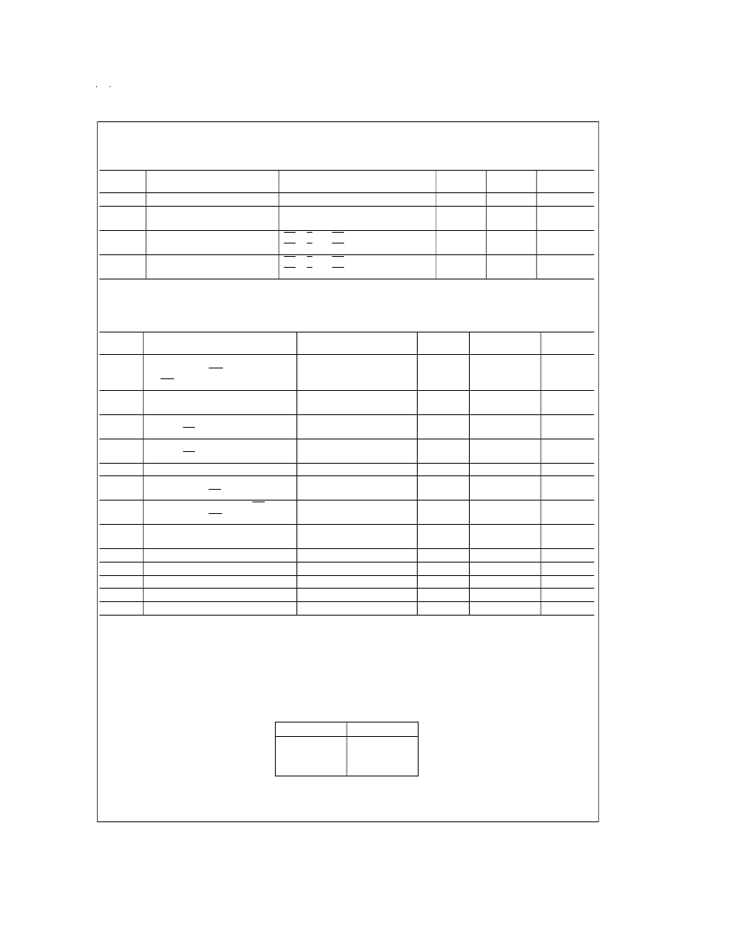
DC Electrical Characteristics
(Continued)
The following specifications apply for V
+
= +5V, V
REF(+)
= 5V V
REF()
= GND, and Speed Adjust pin unconnected unless other-
wise specified.
Boldface limits apply for T
A
= T
J
MIN
to T
MAX
all other limits T
A
= T
J
= +25C.
Symbol
Parameter
Conditions
Typical
(Note 7)
Limit
(Note 8)
0.4
50
50
Units
(Limit)
V (max)
μA (max)
μA (max)
mA (max)
mA (max)
mA (max)
mA (max)
V
OUT(0)
I
OUT
Logical “0” Output Voltage
TRI-STATE
Output Current
V
+
= 4.5V, I
OUT
= 1.6 mA
V
OUT
= 5V
V
OUT
= 0V
CS = S/H = RD = 0, R
SA
=
∞
CS = S/H = RD = 0, R
SA
= 18 k
CS = S/H = RD = 0, R
SA
=
∞
CS = S/H = RD = 0, R
SA
= 18 k
0.1
0.1
1.0
1.0
30
30
DI
CC
DV
CC
Supply Current
2
AI
CC
AV
CC
Supply Current
45
AC Electrical Characteristics
The following specifications apply for V
+
= +5V, t
= t
= 20 ns, V
REF(+)
= 5V, V
= GND, and Speed Adjust pin uncon-
nected unless otherwise specified.
Boldface limits apply for T
A
J
= T
MIN
to T
MAX
;
all other limits T
A
= T
J
= +25C.
Symbol
Parameter
Conditions
Typical
(Note 7)
600
375
Limit
(Note 8)
750/
900
Units
(Limit)
t
CONV
Mode 1 Conversion Time from
Rising Edge of S/H to Falling Edge
of INT
Mode 2 Conversion Time
R
SA
=
∞
R
SA
= 18k
ns(max)
ns
t
CRD
R
SA
=
∞
Mode 2, R
SA
= 18k
Mode 1; C
L
= 100 pF
850
530
1400
ns(max)
ns
t
ACC1
Access Time (Delay from Falling
Edge of RD to Output Valid)
Access Time (Delay from Falling
Edge of RD to Output Valid)
Minimum Sample Time
TRI-STATE Control (Delay from
Rising Edge of RD to High-Z State)
Delay from Rising Edge of RD to
Rising Edge of INT
Delay from End of Conversion to
Next Conversion
Multiplexer Control Setup Time
Multiplexer Hold Time
Analog Input Capacitance
Logic Output Capacitance
Logic Input Capacitance
30
60
ns (max)
t
ACC2
Mode 2; C
L
= 100 pF
900
t
CRD
+ 50
ns (max)
t
SH
t
1H
, t
0H
(Figure 1); (Note 8)
R
L
= 1k, C
L
= 10 pF
250
ns (max)
30
60
ns (max)
t
INTH
C
L
= 100 pF
25
50
ns (max)
t
P
50
ns (max)
t
MS
t
MH
C
VIN
C
OUT
C
IN
10
10
35
5
5
75
40
ns (max)
ns (max)
pF (max)
pF (max)
pF (max)
Note 1:
Absolute Maximum Ratings indicate limits beyond which damage to the device may occur. Operating Ratings indicate conditions for which the device is func-
tional. These ratings do not guarantee specific performance limits, however. For guaranteed specifications and test conditions, see the Electrical Characteristics. The
guaranteed specifications apply only for the test conditions listed. Some performance characteristics may degrade when the device is not operated under the listed
test conditons.
Note 2:
All voltages are measured with respect to GND, unless otherwise specified.
Note 3:
When the input voltage (V
) at any pin exceeds the power supply rails (V
<
GND or V
>
V
+
) the absolute value of current at that pin should be limited
to 5 mA or less. The 20 mA package input current limits the number of pins that can safely exceed the power supplies with an input current of 5 mA to four.
Note 4:
The maximum power dissipation must be derated at elevated temperatures and is dictated by T
,
θ
and the ambient temperature, T
. The maximum
allowable power dissipation at any temperature is P
D
= (T
JMAX
T
A
)/
θ
JA
or the number given in the Absolute Maximum Ratings, whichever is lower. In most cases,
the maximum derated power dissipation will be reached only during fault conditions. For these devices, T
JMAX
for a board-mounted device can be found from the
tables below:
Device
θ
JA
(C/W)
54
48
44
ADC10061CIWM
ADC10062CIWM
ADC10064CIWM
Note 5:
Human body model, 100 pF discharged through a 1.5 k
resistor.
Note 6:
See AN-450 “Surface Mounting Methods and Their Effect on Product Reliability” or the section titled “Surface Mount” found in a current National Semicon-
ductor Linear Data Book for other methods of soldering surface mount devices.
Note 7:
Typicals are at +25C and represent must likely parametric norm.
www.national.com
5
相關(guān)PDF資料 |
PDF描述 |
|---|---|
| ADC10065 | ADC10065 10-Bit 65 MSPS 3V A/D Converter |
| ADC10065CIMT | ADC10065 10-Bit 65 MSPS 3V A/D Converter |
| ADC10065CIMTX | ADC10065 10-Bit 65 MSPS 3V A/D Converter |
| ADC10080CIMTX | 10-Bit, 80 MSPS, 3V, 78.6 mW A/D Converter |
| ADC10080CIMT | 10-Bit, 80 MSPS, 3V, 78.6 mW A/D Converter |
相關(guān)代理商/技術(shù)參數(shù) |
參數(shù)描述 |
|---|---|
| ADC10064CIWM/NOPB | 功能描述:模數(shù)轉(zhuǎn)換器 - ADC RoHS:否 制造商:Texas Instruments 通道數(shù)量:2 結(jié)構(gòu):Sigma-Delta 轉(zhuǎn)換速率:125 SPs to 8 KSPs 分辨率:24 bit 輸入類型:Differential 信噪比:107 dB 接口類型:SPI 工作電源電壓:1.7 V to 3.6 V, 2.7 V to 5.25 V 最大工作溫度:+ 85 C 安裝風(fēng)格:SMD/SMT 封裝 / 箱體:VQFN-32 |
| ADC10064CIWMX | 功能描述:模數(shù)轉(zhuǎn)換器 - ADC RoHS:否 制造商:Texas Instruments 通道數(shù)量:2 結(jié)構(gòu):Sigma-Delta 轉(zhuǎn)換速率:125 SPs to 8 KSPs 分辨率:24 bit 輸入類型:Differential 信噪比:107 dB 接口類型:SPI 工作電源電壓:1.7 V to 3.6 V, 2.7 V to 5.25 V 最大工作溫度:+ 85 C 安裝風(fēng)格:SMD/SMT 封裝 / 箱體:VQFN-32 |
| ADC10064CIWMX/NOPB | 功能描述:模數(shù)轉(zhuǎn)換器 - ADC RoHS:否 制造商:Texas Instruments 通道數(shù)量:2 結(jié)構(gòu):Sigma-Delta 轉(zhuǎn)換速率:125 SPs to 8 KSPs 分辨率:24 bit 輸入類型:Differential 信噪比:107 dB 接口類型:SPI 工作電源電壓:1.7 V to 3.6 V, 2.7 V to 5.25 V 最大工作溫度:+ 85 C 安裝風(fēng)格:SMD/SMT 封裝 / 箱體:VQFN-32 |
| ADC10064CIWMXNOPB | 制造商:National Semiconductor 功能描述:ADC Single Pipelined 800ksps 10-bit Parallel 28-Pin SOIC W T/R |
| ADC10064CMJ | 制造商:未知廠家 制造商全稱:未知廠家 功能描述:Single-Ended Data Acquisition System |
發(fā)布緊急采購(gòu),3分鐘左右您將得到回復(fù)。