- 您現(xiàn)在的位置:買賣IC網(wǎng) > PDF目錄373963 > AD9446BSVZ-100 (ANALOG DEVICES INC) 16-Bit, 80/100 MSPS ADC PDF資料下載
參數(shù)資料
| 型號(hào): | AD9446BSVZ-100 |
| 廠商: | ANALOG DEVICES INC |
| 元件分類: | ADC |
| 英文描述: | 16-Bit, 80/100 MSPS ADC |
| 中文描述: | 1-CH 16-BIT PROPRIETARY METHOD ADC, PARALLEL ACCESS, PQFP100 |
| 封裝: | EXPOSEDPAD, LEAD FREE, PLASTIC, MS-026-AED, TQFP-44 |
| 文件頁數(shù): | 6/36頁 |
| 文件大小: | 952K |
| 代理商: | AD9446BSVZ-100 |
第1頁第2頁第3頁第4頁第5頁當(dāng)前第6頁第7頁第8頁第9頁第10頁第11頁第12頁第13頁第14頁第15頁第16頁第17頁第18頁第19頁第20頁第21頁第22頁第23頁第24頁第25頁第26頁第27頁第28頁第29頁第30頁第31頁第32頁第33頁第34頁第35頁第36頁
AD9446
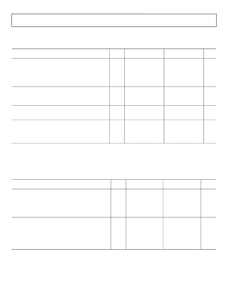
DIGITAL SPECIFICATIONS
AVDD1 = 3.3 V, AVDD2 = 5.0 V, DRVDD = 3.3 V, R
LVDS_BIAS
= 3.74 kΩ, unless otherwise noted.
Table 3.
Parameter
CMOS LOGIC INPUTS (DFS, DCS MODE, OUTPUT MODE)
High Level Input Voltage
Low Level Input Voltage
High Level Input Current
Low Level Input Current
Input Capacitance
DIGITAL OUTPUT BITS—CMOS MODE (D0 to D15, OTR)
1
DRVDD = 3.3 V
High Level Output Voltage
Low Level Output Voltage
DIGITAL OUTPUT BITS—LVDS MODE (D0 to D15, OTR)
V
OD
Differential Output Voltage
2
V
OS
Output Offset Voltage
CLOCK INPUTS (CLK+, CLK)
Differential Input Voltage
Common-Mode Voltage
Input Resistance
Input Capacitance
1
Output voltage levels measured with 5 pF load on each output.
2
LVDS R
TERM
= 100 Ω.
Rev. 0 | Page 6 of 36
Temp
Full
Full
Full
Full
Full
Full
Full
Full
Full
Full
Full
Full
Full
AD9446BSVZ-80
Min
Typ
2.0
10
2
3.25
247
1.125
0.2
1.3
1.5
1.1
1.4
2
AD9446BSVZ-100
Min
Typ
2.0
10
2
3.25
247
1.125
0.2
1.3
1.5
1.1
1.4
2
Unit
V
V
μA
μA
pF
V
V
mV
V
V
V
kΩ
pF
Max
0.8
200
+10
0.2
545
1.375
1.6
1.7
Max
0.8
200
+10
0.2
545
1.375
1.6
1.7
SWITCHING SPECIFICATIONS
AVDD1 = 3.3 V, AVDD2 = 5.0 V, DRVDD = 3.3 V, unless otherwise noted.
Table 4.
Parameter
CLOCK INPUT PARAMETERS
Maximum Conversion Rate
Minimum Conversion Rate
CLK Period
CLK Pulse Width High
1
(t
CLKH
)
CLK Pulse Width Low
1
(t
CLKL
)
DATA OUTPUT PARAMETERS
Output Propagation Delay—CMOS (t
PD
)
2
(Dx, DCO+)
Output Propagation Delay—LVDS (t
PD
)
3
(Dx+), (t
CPD
)
3
(DCO+)
Pipeline Delay (Latency)
Aperture Delay (t
A
)
Aperture Uncertainty (Jitter, t
J
)
Temp
Full
Full
Full
Full
Full
Full
Full
Full
Full
Full
AD9446BSVZ-80
Min
Typ
80
12.5
5.0
5.0
3.35
2.1
3.6
13
60
AD9446BSVZ-100
Min
Typ
100
10
4.0
4.0
3.35
2.3
3.6
13
60
Unit
MSPS
MSPS
ns
ns
ns
ns
ns
Cycles
ns
fsec
rms
Max
1
4.8
Max
1
4.8
1
With duty cycle stabilizer (DCS) enabled.
2
Output propagation delay is measured from clock 50% transition to data 50% transition with 5 pF load.
3
LVDS R
TERM
= 100 Ω. Measured from the 50% point of the rising edge of CLK+ to the 50% point of the data transition.
相關(guān)PDF資料 |
PDF描述 |
|---|---|
| AD9446BSVZ-80 | 16-Bit, 80/100 MSPS ADC |
| AD9446 | 16-Bit, 80/100 MSPS ADC |
| AD9446-100LVDS | 16-Bit, 80/100 MSPS ADC |
| AD9446-100PCB | 16-Bit, 80/100 MSPS ADC |
| AD9446-80LVDS | 16-Bit, 80/100 MSPS ADC |
相關(guān)代理商/技術(shù)參數(shù) |
參數(shù)描述 |
|---|---|
| AD9446BSVZ-1001 | 制造商:AD 制造商全稱:Analog Devices 功能描述:16-Bit, 80/100 MSPS ADC |
| AD9446BSVZ-105 | 制造商:Analog Devices 功能描述:- Bulk |
| AD9446BSVZ-80 | 功能描述:模數(shù)轉(zhuǎn)換器 - ADC 16Bit 80 MSPS ADC PB Free RoHS:否 制造商:Analog Devices 通道數(shù)量: 結(jié)構(gòu): 轉(zhuǎn)換速率: 分辨率: 輸入類型: 信噪比: 接口類型: 工作電源電壓: 最大工作溫度: 安裝風(fēng)格: 封裝 / 箱體: |
| AD9446BSVZ-801 | 制造商:AD 制造商全稱:Analog Devices 功能描述:16-Bit, 80/100 MSPS ADC |
| AD9446XSVZ-80 | 制造商:Analog Devices 功能描述:16-BIT, 100 MSPS ADC - Bulk |
發(fā)布緊急采購,3分鐘左右您將得到回復(fù)。