- 您現(xiàn)在的位置:買(mǎi)賣(mài)IC網(wǎng) > PDF目錄362110 > AD840SQ-883B (ANALOG DEVICES INC) Wideband, Fast Settling Op Amp PDF資料下載
參數(shù)資料
| 型號(hào): | AD840SQ-883B |
| 廠商: | ANALOG DEVICES INC |
| 元件分類(lèi): | 運(yùn)動(dòng)控制電子 |
| 英文描述: | Wideband, Fast Settling Op Amp |
| 中文描述: | OP-AMP, 2000 uV OFFSET-MAX, 400 MHz BAND WIDTH, CDIP14 |
| 封裝: | HERMETIC SEALED, CERDIP-14 |
| 文件頁(yè)數(shù): | 8/20頁(yè) |
| 文件大小: | 463K |
| 代理商: | AD840SQ-883B |
第1頁(yè)第2頁(yè)第3頁(yè)第4頁(yè)第5頁(yè)第6頁(yè)第7頁(yè)當(dāng)前第8頁(yè)第9頁(yè)第10頁(yè)第11頁(yè)第12頁(yè)第13頁(yè)第14頁(yè)第15頁(yè)第16頁(yè)第17頁(yè)第18頁(yè)第19頁(yè)第20頁(yè)
REV. C
AD8400/AD8402/AD8403
–8–
AD8400 PIN FUNCTION DESCRIPTIONS
Pin
Name
Description
1
2
3
B1
GND
CS
Terminal B RDAC
Ground
Chip Select Input, Active Low. When
CS
returns high, data in the serial input register
is loaded into the DAC register.
Serial Data Input
Serial Clock Input, Positive Edge Triggered.
Positive power supply, specified for operation
at both 3 V and 5 V.
Wiper RDAC, Addr = 00
2
Terminal A RDAC
4
5
6
SDI
CLK
V
DD
7
8
W1
A1
AD8402 PIN FUNCTION DESCRIPTIONS
Pin
Name
Description
1
2
3
4
5
6
AGND
B2
A2
W2
DGND
SHDN
Analog Ground
*
Terminal B RDAC #2
Terminal A RDAC #2
Wiper RDAC #2, Addr = 01
2
.
Digital Ground
*
Terminal A Open Circuit. Shutdown controls
Variable Resistors #1 and #2.
Chip Select Input, Active Low. When
CS
returns high, data in the serial input register is
decoded based on the address bits and loaded
into the target DAC register.
Serial Data Input
Serial Clock Input, Positive Edge Triggered.
Active low reset to midscale; sets RDAC
registers to 80
H
.
Positive power supply, specified for operation
at both 3 V and 5 V.
Wiper RDAC #1, Addr = 00
2
.
Terminal A RDAC #1
Terminal B RDAC #1
7
CS
8
9
10
SDI
CLK
RS
11
V
DD
12
13
14
W1
A1
B1
*
All AGNDs must be connected to DGND.
AD8403 PIN FUNCTION DESCRIPTIONS
Pin
Name
Description
1
2
3
4
5
6
7
8
9
10
AGND2
B2
A2
W2
AGND4
B4
A4
W4
DGND
SHDN
Analog Ground #2
*
Terminal B RDAC #2
Terminal A RDAC #2
Wiper RDAC #2, Addr = 01
2
.
Analog Ground #4
*
Terminal B RDAC #4
Terminal A RDAC #4
Wiper RDAC #4, Addr = 11
2
.
Digital Ground
*
Active Low Input. Terminal A open circuit.
Shutdown controls Variable Resistors #1
through #4.
Chip Select Input, Active Low. When
CS
returns high, data in the serial input register
is decoded based on the address bits and
loaded into the target DAC register.
Serial Data Input
Serial Data Output, Open Drain transistor
requires pull-up resistor.
Serial Clock Input, Positive Edge Triggered
Active Low reset to midscale; sets RDAC
registers to 80
H
.
Positive power supply, specified for
operation at both 3 V and 5 V.
Analog Ground #3
*
Wiper RDAC #3, Addr = 10
2
Terminal A RDAC #3
Terminal B RDAC #3
Analog Ground #1
*
Wiper RDAC #1, Addr = 00
2
Terminal A RDAC #1
Terminal B RDAC #1
11
CS
12
13
SDI
SDO
14
15
CLK
RS
16
V
DD
17
18
19
20
21
22
23
24
AGND3
W3
A3
B3
AGND1
W1
A1
B1
*
All AGNDs must be connected to DGND.
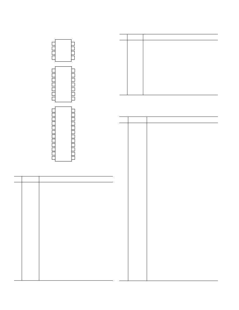
PIN CONFIGURATIONS
1
2
3
4
8
7
6
5
TOP VIEW
(Not to Scale)
AD8400
B1
CLK
V
DD
W1
A1
GND
CS
SDI
14
13
12
11
10
9
8
1
2
3
4
7
6
5
TOP VIEW
(Not to Scale)
AGND
V
DD
RS
W1
A1
B1
B2
A2
W2
AD8402
SDI
CLK
DGND
SHDN
CS
13
16
15
14
24
23
22
21
20
19
18
17
TOP VIEW
(Not to Scale)
12
11
10
9
8
1
2
3
4
7
6
5
AD8403
AGND2
AGND1
W1
A1
B1
B2
A2
W2
W3
A3
B3
AGND4
B4
A4
W4
DGND
SHDN
RS
V
DD
AGND3
CS
SDI
CLK
SDO
相關(guān)PDF資料 |
PDF描述 |
|---|---|
| AD840 | Wideband, Fast Settling Op Amp |
| AD840JN | Wideband, Fast Settling Op Amp |
| AD840JQ | Wideband, Fast Settling Op Amp |
| AD840KN | Wideband, Fast Settling Op Amp |
| AD840KQ | Wideband, Fast Settling Op Amp |
相關(guān)代理商/技術(shù)參數(shù) |
參數(shù)描述 |
|---|---|
| AD841 | 制造商:AD 制造商全稱(chēng):Analog Devices 功能描述:Wideband, Unity-Gain Stable, Fast Settling Op Amp |
| AD841-0026 | 制造商:Analog Devices 功能描述: |
| AD8417 | 制造商:AD 制造商全稱(chēng):Analog Devices 功能描述:Bidirectional, Zero Drift, Current Sense Amplifier |
| AD8417BRMZ | 制造商:Analog Devices 功能描述:DMOS CSAMP G=60 80V BIDIR 0 DRIFT - Rail/Tube 制造商:Analog Devices 功能描述:IC OPAMP CURR SENSE 8MSOP |
| AD8417BRMZ-RL | 制造商:Analog Devices 功能描述:DMOS CSAMP G=60 80V BIDIR 0 DRIFT - Tape and Reel |
發(fā)布緊急采購(gòu),3分鐘左右您將得到回復(fù)。