- 您現(xiàn)在的位置:買賣IC網(wǎng) > PDF目錄375243 > AD8310-EVAL (Analog Devices, Inc.) Fast, Voltage-Out DC-440 MHz 95 dB Logarithmic Amplifier PDF資料下載
參數(shù)資料
| 型號(hào): | AD8310-EVAL |
| 廠商: | Analog Devices, Inc. |
| 元件分類: | 運(yùn)動(dòng)控制電子 |
| 英文描述: | Fast, Voltage-Out DC-440 MHz 95 dB Logarithmic Amplifier |
| 中文描述: | 快速,電壓輸出的DC - 440 MHz的95分貝數(shù)放大器 |
| 文件頁數(shù): | 16/16頁 |
| 文件大?。?/td> | 323K |
| 代理商: | AD8310-EVAL |
–16–
C
P
AD8310
REV. A
Table III. Evaluation Boards Setup Options
Component
TP1, TP2
SW1
Function
Supply and Ground Vector Pins
Device Enable: When in Position A, the ENBL pin is connected to +V
S
and the
AD8310 is in normal operating mode. In Position B, the ENBL pin is connected to
ground putting the device in sleep mode.
SMA Connector Grounds: Connects common of INHI and INLO SMA connectors
to ground. Can be used to isolate the generator ground from the evaluation board
ground (see Figure 26).
Input Interface: R3 (52.3
) combines with the AD8310’s 1 k
input impedance to
give an overall broadband input impedance of 50
. C1, C2, and the AD8310’s input
impedance combine to set a high-pass input corner of 32 kHz. Alternatively, R3, C1,
and C2 can be replaced by an inductor and matching capacitors to form an input
matching network. See Input Matching section for more detail.
RSSI (Video) Bandwidth Adjust: The addition of C3 (Farads) will lower the RSSI bandwidth
of the VLOG output according to the equation: C
FILT
= 1/(2
π ×
3 k
×
Video Bandwidth)
–2.1 pF.
Supply Decoupling: The nominal supply decoupling of 0.01
μ
F (C4) can be augmented by a
larger cap in C5. An inductor or small resistor can be placed in R5 for additional decoupling.
Output Source Impedance: In cable-driving applications, a resistor (typically 50
or 75
)
can be placed in R6 to give the circuit a back-terminated output impedance.
Output Loading: Resistors and capacitors can be placed in C6 and R7 to load test V
OUT
.
Jumpers W1 and W2 are used to connect/disconnect the loads.
Offset Compensation Loop:
A capacitor in C7 will reduce the corner frequency of
the offset control loop in low frequency applications.
Default Condition
Not Applicable
SW1 = A
R1/R4
R1 = R4 = 0
C1, C2, R2, R3
R3 = 52.3
R2 = 0
C1 = C2 = 0.01
μ
F
C3
C3 = Open
C4, C5, R5
C4 = 0.01
μ
F
C5 = Open, R5 = 0
R6 = 0
R6
W1, W2, C6, R7
C6 = R7 = Open
W1 = W2 = Installed
C7 = Open
C7
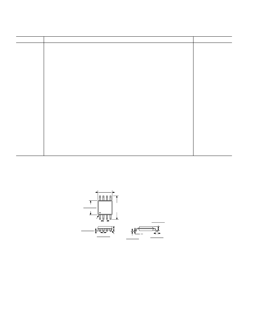
OUTLINE DIMENSIONS
Dimensions shown in inches and (mm).
8-Lead Mini_SO
(RM-8)
0.009 (0.23)
0.005 (0.13)
0.028 (0.70)
0.016 (0.40)
6
8
0
8
0.037 (0.95)
0.030 (0.75)
8
5
4
1
0.122 (3.10)
0.114 (2.90)
PIN 1
0.0256 (0.65) BSC
0.122 (3.10)
0.114 (2.90)
0.193
(4.90)
BSC
SEATING
PLANE
0.006 (0.15)
0.002 (0.05)
0.016 (0.40)
0.010 (0.25)
0.043
(1.10)
MAX
相關(guān)PDF資料 |
PDF描述 |
|---|---|
| AD8310ARM | Fast, Voltage-Out DC-440 MHz 95 dB Logarithmic Amplifier |
| AD8310ARM-REEL | Fast, Voltage-Out DC-440 MHz 95 dB Logarithmic Amplifier |
| AD8310ARM-REEL7 | Fast, Voltage-Out DC-440 MHz 95 dB Logarithmic Amplifier |
| AD8315 | 50 dB GSM PA Controller |
| AD8315-EVAL | 50 dB GSM PA Controller |
相關(guān)代理商/技術(shù)參數(shù) |
參數(shù)描述 |
|---|---|
| AD8310-EVALZ | 功能描述:BOARD EVAL FOR AD8310 RoHS:是 類別:編程器,開發(fā)系統(tǒng) >> 評(píng)估板 - 運(yùn)算放大器 系列:- 產(chǎn)品培訓(xùn)模塊:Lead (SnPb) Finish for COTS Obsolescence Mitigation Program 標(biāo)準(zhǔn)包裝:1 系列:- |
| AD8311 | 制造商:AD 制造商全稱:Analog Devices 功能描述:50 dB GSM PA Controller |
| AD8311ACBZ-P2 | 制造商:Analog Devices 功能描述:GSM PA CNTRLR 6PIN WLCSP - Tape and Reel |
| AD8311ACBZ-P7 | 功能描述:IC CTRLR PWR AMP 2.5GHZ 6WLCSP RoHS:是 類別:RF/IF 和 RFID >> RF 電源控制器 IC 系列:- 標(biāo)準(zhǔn)包裝:3,000 系列:- RF 型:GSM 頻率:450MHz ~ 2GHz 特點(diǎn):四頻帶 封裝/外殼:8-VFBGA 供應(yīng)商設(shè)備封裝:8-MicroSMD(1.51x1.51) 包裝:帶卷 (TR) 其它名稱:LMV243BLX |
| AD8311-EVAL | 制造商:Analog Devices 功能描述:50 DB GSM PA CNTRLR - Bulk |
發(fā)布緊急采購,3分鐘左右您將得到回復(fù)。