- 您現(xiàn)在的位置:買賣IC網(wǎng) > PDF目錄375239 > AD7816 (Analog Devices, Inc.) 10-Bit ADCs with On-Chip Temperature Sensor(10位A/D轉(zhuǎn)換器) PDF資料下載
參數(shù)資料
| 型號: | AD7816 |
| 廠商: | Analog Devices, Inc. |
| 元件分類: | 溫度/濕度傳感器 |
| 英文描述: | 10-Bit ADCs with On-Chip Temperature Sensor(10位A/D轉(zhuǎn)換器) |
| 中文描述: | 10位ADC的片上溫度傳感器(10位的A / D轉(zhuǎn)換器) |
| 文件頁數(shù): | 6/16頁 |
| 文件大?。?/td> | 230K |
| 代理商: | AD7816 |
AD7816/AD7817/AD7818
–6–
REV. 0
CAUTION
ESD (electrostatic discharge) sensitive device. Electrostatic charges as high as 4000 V readily
accumulate on the human body and test equipment and can discharge without detection.
Although the
AD7816/AD7817/AD7818
feature proprietary ESD protection circuitry, perma-
nent damage may occur on devices subjected to high energy electrostatic discharges. Therefore,
proper ESD precautions are recommended to avoid performance degradation or loss of functionality.
ABSOLUTE MAXIMUM RATINGS
1
(
T
A
= +25
°
C unless otherwise noted)
V
DD
to AGND . . . . . . . . . . . . . . . . . . . . . . . . . –0.3V to +7V
V
DD
to DGND . . . . . . . . . . . . . . . . . . . . . . . . . –0.3V to +7V
Analog Input Voltage to AGND
VIN1 to VIN4 . . . . . . . . . . . . . . . . . –0.3 V to V
DD
+ 0.3 V
Reference Input Voltage to AGND
2
. . . –0.3 V to V
DD
+ 0.3V
Digital Input Voltage to DGND . . . . . . –0.3 V to V
DD
+ 0.3 V
Digital Output Voltage to DGND . . . . . –0.3 V to V
DD
+ 0.3 V
Storage Temperature Range . . . . . . . . . . . . –65
°
C to +150
°
C
Junction Temperature . . . . . . . . . . . . . . . . . . . . . . . . . +150
°
C
TSSOP, Power Dissipation . . . . . . . . . . . . . . . . . . . . 450 mW
θ
JA
Thermal Impedance . . . . . . . . . . . . . . . . . . . . . 120
°
C/W
Lead Temperature, Soldering . . . . . . . . . . . . . . . . . +260
°
C
Vapor Phase (60 sec) . . . . . . . . . . . . . . . . . . . . . . +215
°
C
Infrared (15 sec) . . . . . . . . . . . . . . . . . . . . . . . . . +220
°
C
16-Lead SOIC Package, Power Dissipation . . . . . . . . 450 mW
θ
JA
Thermal Impedance . . . . . . . . . . . . . . . . . . . . . 100
°
C/W
Lead Temperature, Soldering
Vapor Phase (60 sec) . . . . . . . . . . . . . . . . . . . . . . +215
°
C
Infrared (15 sec) . . . . . . . . . . . . . . . . . . . . . . . . . +220
°
C
8-Lead SOIC Package, Power Dissipation . . . . . . . . . 450 mW
θ
JA
Thermal Impedance . . . . . . . . . . . . . . . . . . . . . 157
°
C/W
Lead Temperature, Soldering
Vapor Phase (60 sec) . . . . . . . . . . . . . . . . . . . . . . +215
°
C
Infrared (15 sec) . . . . . . . . . . . . . . . . . . . . . . . . . +220
°
C
ORDERING GUIDE
Temperature
Range
Temperature
Error @ +25
°
C
Package
Description
Branding
Information
Package
Options
Model
AD7816AR
AD7816ARM
AD7817AR
AD7817BR
AD7817ARU
AD7817BRU
AD7817SR
AD7818AR
AD7818ARM
–55
°
C to +125
°
C
–55
°
C to +125
°
C
–40
°
C to +85
°
C
–40
°
C to +85
°
C
–40
°
C to +85
°
C
–40
°
C to +85
°
C
–55
°
C to +125
°
C
–55
°
C to +125
°
C
–55
°
C to +125
°
C
±
2
°
C
±
2
°
C
±
2
°
C
±
1
°
C
±
2
°
C
±
1
°
C
±
2
°
C
±
2
°
C
±
2
°
C
8-Lead Narrow Body (SOIC)
8-Lead
μ
SOIC
16-Lead Narrow Body (SOIC)
16-Lead Narrow Body (SOIC)
16-Lead (TSSOP)
16-Lead (TSSOP)
16-Lead Narrow Body (SOIC)
8-Lead Narrow Body (SOIC)
8-Lead
μ
SOIC
SO-8
RM-8
R-16A
R-16A
RU-16
RU-16
R-16A
SO-8
RM-8
C4A
C3A
μ
SOIC Package, Power Dissipation . . . . . . . . . . . . . . 450 mW
θ
JA
Thermal Impedance . . . . . . . . . . . . . . . . . . . . . 206
°
C/W
Lead Temperature, Soldering
Vapor Phase (60 sec) . . . . . . . . . . . . . . . . . . . . . . +215
°
C
Infrared (15 sec) . . . . . . . . . . . . . . . . . . . . . . . . . +220
°
C
NOTES
1
Stresses above those listed under Absolute Maximum Ratings may cause perma-
nent damage to the device. This is a stress rating only; functional operation of the
device at these or any other conditions above those listed in the operational sections
of this specification is not implied. Exposure to absolute maximum rating condi-
tions for extended periods may affect device reliability.
2
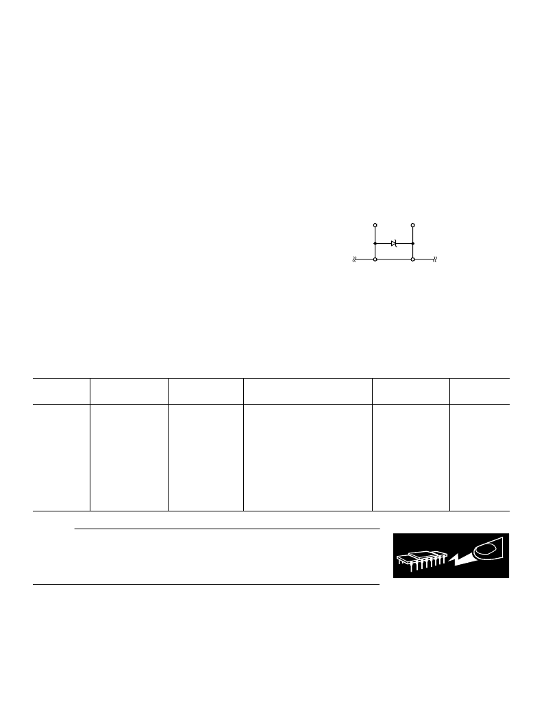
If the Reference Input Voltage is likely to exceed V
DD
by more than 0.3 V (e.g.,
during power-up) and the reference is capable of supplying 30 mA or more, it is
recommended to use a clamping diode between the REF
IN
pin and V
DD
pin. The
diagram below shows how the diode should be connected.
REF
IN
V
DD
BAT81
AD7816/AD7817
WARNING!
ESD SENSITIVE DEVICE
相關(guān)PDF資料 |
PDF描述 |
|---|---|
| AD7817 | 10-Bit ADCs with On-Chip Temperature Sensor(四通道,10位A/D轉(zhuǎn)換器) |
| AD7818 | 10-Bit ADCs with On-Chip Temperature Sensor(單通道,10位A/D轉(zhuǎn)換器) |
| AD7819 | 8-Bit Sampling ADC(200kSPS,8位采樣A/D轉(zhuǎn)換器) |
| AD7820 | LC2MOS HIGH-SPEED uP-COMPATIBLE 8-BIT ADC WITH TRACK/HOLD FUNCTION |
| AD7820BQ | LC2MOS HIGH-SPEED uP-COMPATIBLE 8-BIT ADC WITH TRACK/HOLD FUNCTION |
相關(guān)代理商/技術(shù)參數(shù) |
參數(shù)描述 |
|---|---|
| AD7816-7818 | 制造商:AD 制造商全稱:Analog Devices 功能描述:Single- and 4-Channel, 9 us, 10-Bit ADCs with On-Chip Temperature Sensor |
| AD7816ACHIPS | 制造商:AD 制造商全稱:Analog Devices 功能描述:Single- and 4-Channel, 9 us, 10-Bit ADCs with On-Chip Temperature Sensor |
| AD7816AR | 制造商:Analog Devices 功能描述:Analog Temperature Sensors 8-Pin SOIC N 制造商:Rochester Electronics LLC 功能描述:TEMP SENSOR I.C. - Bulk 制造商:Analog Devices 功能描述:ADC TEMP SENSOR SMD 7816 SOIC8 |
| AD7816ARM | 制造商:Analog Devices 功能描述:Analog Temperature Sensors 8-Pin MSOP 制造商:Rochester Electronics LLC 功能描述:TEMPERATURE SENSOR: 10-BIT ADC, TEMPERATURE MONITORING ONLY - Bulk |
| AD7816ARM-REEL | 制造商:Analog Devices 功能描述:Analog Temperature Sensors 8-Pin MSOP T/R 制造商:Rochester Electronics LLC 功能描述:TEMPERATURE SENSOR: 10-BIT ADC, TEMPERATURE MONITORING ONLY - Tape and Reel |
發(fā)布緊急采購,3分鐘左右您將得到回復(fù)。