- 您現(xiàn)在的位置:買賣IC網(wǎng) > PDF目錄362103 > AD744BQ (ANALOG DEVICES INC) Precision, 500 ns Settling BiFET Op Amp PDF資料下載
參數(shù)資料
| 型號: | AD744BQ |
| 廠商: | ANALOG DEVICES INC |
| 元件分類: | 運動控制電子 |
| 英文描述: | Precision, 500 ns Settling BiFET Op Amp |
| 中文描述: | OP-AMP, 1000 uV OFFSET-MAX, 13 MHz BAND WIDTH, CDIP8 |
| 封裝: | CERDIP-8 |
| 文件頁數(shù): | 16/24頁 |
| 文件大小: | 914K |
| 代理商: | AD744BQ |
REV. PrF
PRELIMINARY TECHNICAL DATA
–16–
AD7450A/AD7440
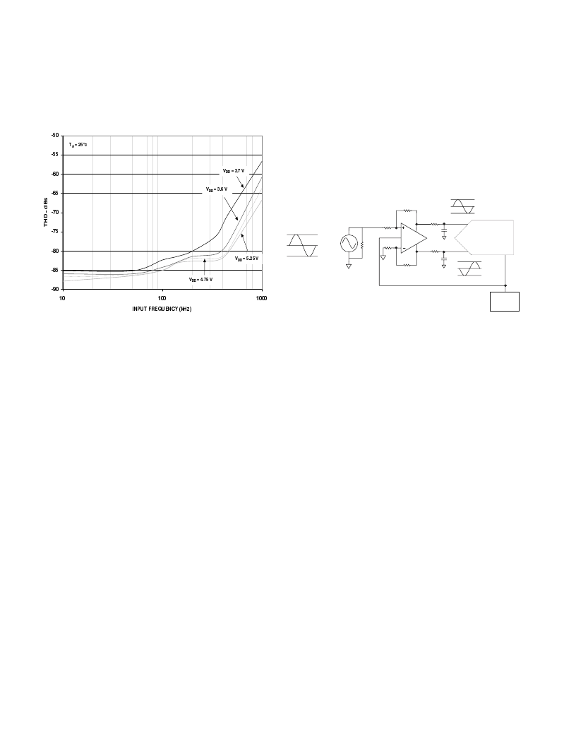
Figure 14 shows a graph of THD versus analog input
frequency for V
DD
of 5 V ± 5% and 3 V +20/-10%, while
sampling at 1MSPS with a SCLK of 18 MHz. In this
case the source impedance is 10 .
Figure 14.THD vs Analog Input Frequency for 3V and 5V
Supply Voltages
DRIVING DIFFERENTIAL INPUTS
Differential operation requires that V
IN+
and V
IN-
be si-
multaneously driven with two equal signals that are 180
o
out of phase. The common mode must be set up exter-
nally and has a range which is determined by V
REF
, the
power supply and the particular amplifier used to drive the
analog inputs (see figures 9 and 10). Differential modes
of operation with either an ac or dc input, provide the best
THD performance over a wide frequency range. Since
not all applications have a signal preconditioned for differ-
ential operation, there is often a need to perform single
ended to differential conversion.
Differential Amplifier
An ideal method of applying differential drive to the AD7450A/
AD7440 is to use a differential amplifier such as the AD8138.
This part can be used as a single ended to differential
amplifier or as a differential to differential amplifier. In both
cases the analog input needs to be bipolar. It also provides
common mode level shifting and buffering of the bipolar
input signal. Figure 15 shows how the AD8138 can be used
as a single ended to differential amplifier. The positive and
negative outputs of the AD8138 are connected to the respec-
tive inputs on the ADC via a pair of series resistors to
minimize the effects of switched capacitance on the front end
of the ADCs. The RC low pass filter on each analog input
is recommended in ac applications to remove high frequency
components of the analog input. The architecture of the
AD8138 results in outputs that are very highly balanced over
a wide frequency range without requiring tightly matched
external components.
If the analog input source being used has zero impedance then
all four resistors (Rg1, Rg2, Rf1, Rf2) should be the same. If
the source has a 50
impedance and a 50
termination for
example, the value of Rg2 should be increased by 25
to
balance this parallel impedance on the input and thus ensure
that both the positive and negative analog inputs have the
same gain (see figure 15). The outputs of the amplifier are
perfectly matched, balanced differential outputs of identical
amplitude and are exactly 180
o
out of phase.
The AD8138 is specified with 3 V, 5 V and ±5 V power
supplies but the best results are obtained when it is supplied
by ±5 V. A lower cost device that could also be used in this
configuration with slight differences in characteristics to the
AD8138 but with similar performance and operation is the
AD8132.
2.5V
1.25V
3.75V
Rs*
Rs*
Rf2
2.5V
1.25V
3.75V
EXTERNAL
VREF (2.5V)
VREF
VIN+
AD7450A/
AD7440
VIN-
AD8138
C*
C*
*Mount as close to the AD7450A/AD7440 as
possible and ensure high
precision Rs and Cs are used
Rs - 50R; C - 1nF;
Rg1=Rf1=Rf2= 499R; Rg2 = 523R
Rf1
Rg1
Vocm
Rg2
51R
GND
+2.5V
-2.5V
Figure 15. Using the AD8138 as a Single Ended to
Differential Amplifier
Opamp Pair
An opamp pair can be used to directly couple a differential
signal to the AD7450A/AD7440. The circuit configura-
tions shown in figures 16(a) and 16(b) show how a dual
opamp can be used to convert a single ended signal into a
differential signal for both a bipolar and a unipolar input
signal respectively.
The voltage applied to point A sets up the Common Mode
Voltage. In both diagrams, it is connected in some way to
the reference but any value in the common mode range
can be input here to setup the common mode. Examples
of suitable dual opamps that could be used in this configu-
ration to provide differential drive to the AD7450A/
AD7440 are the AD8042, AD8056 and the AD8022.
Care must be taken when chosing the opamp used, as the
selection will depend on the required power supply and
the system performance objectives. The driver circuits in
figures 16(a) and 16(b) are optimized for dc coupling
applications requiring optimum distortion performance.
The differential op-amp driver circuit in figure 16(a) is
configured to convert and level shift a single ended,
ground referenced (bipolar) signal to a differential signal
centered at the V
REF
level of the ADC.
The circuit configuration shown in figure 16(b) converts a
unipolar, single ended signal into a differential signal.
相關(guān)PDF資料 |
PDF描述 |
|---|---|
| AD744JR-REEL | Precision, 500 ns Settling BiFET Op Amp |
| AD744JR-REEL7 | Precision, 500 ns Settling BiFET Op Amp |
| AD7477A | AD7476A/AD7477A/AD7478A: 2.35 V to 5.25 V. 1 MSPS. 12-/10-/8-Bit ADCs in 6-Lead SC70 Data Sheet (Rev. A. 2/03) |
| AD7478A | AD7476A/AD7477A/AD7478A: 2.35 V to 5.25 V. 1 MSPS. 12-/10-/8-Bit ADCs in 6-Lead SC70 Data Sheet (Rev. A. 2/03) |
| AD7472 | AD7470/AD7472: 1.75MSPS. 4mW 10-Bit/12-Bit SAR ADC Data Sheet (Rev. A. 3/00) |
相關(guān)代理商/技術(shù)參數(shù) |
參數(shù)描述 |
|---|---|
| AD744BQ/+ | 制造商:Rochester Electronics LLC 功能描述:- Bulk |
| AD744CH | 制造商:Rochester Electronics LLC 功能描述:- Bulk |
| AD744CQ | 制造商:Rochester Electronics LLC 功能描述: 制造商:Analog Devices 功能描述: |
| AD744CQ/+ | 制造商:未知廠家 制造商全稱:未知廠家 功能描述:Voltage-Feedback Operational Amplifier |
| AD744JCHIPS | 制造商:AD 制造商全稱:Analog Devices 功能描述:Precision, 500 ns Settling BiFET Op Amp |
發(fā)布緊急采購,3分鐘左右您將得到回復(fù)。