- 您現(xiàn)在的位置:買賣IC網(wǎng) > PDF目錄373893 > AD7225TQ (ANALOG DEVICES INC) LC2MOS Quad 8-Bit DAC with Separate Reference Inputs PDF資料下載
參數(shù)資料
| 型號: | AD7225TQ |
| 廠商: | ANALOG DEVICES INC |
| 元件分類: | DAC |
| 英文描述: | LC2MOS Quad 8-Bit DAC with Separate Reference Inputs |
| 中文描述: | QUAD, PARALLEL, 8 BITS INPUT LOADING, 8-BIT DAC, CDIP24 |
| 封裝: | CERDIP-24 |
| 文件頁數(shù): | 7/12頁 |
| 文件大小: | 339K |
| 代理商: | AD7225TQ |
AD7225
REV. B
–7–
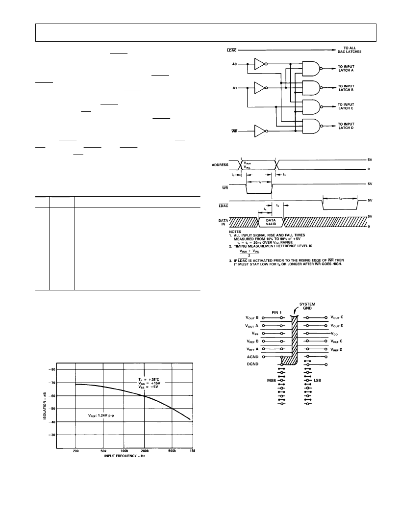
Only the data held in the DAC register determines the analog
output of the converter. T he
LDAC
signal is common to all four
DACs and controls the transfer of information from the input
registers to the DAC registers. Data is latched into all four DAC
registers simultaneously on the rising edge of
LDAC
. T he
LDAC
signal is level triggered and therefore the DAC registers
may be made transparent by tying
LDAC
LOW (in this case the
outputs of the converters will respond to the data held in their
respective input latches).
LDAC
is an asynchronous signal and
is independent of
WR
. T his is useful in many applications.
However, in systems where the asynchronous
LDAC
can occur
during a write cycle (or vice versa) care must be taken to ensure
that incorrect data is not latched through to the output. In other
words, if
LDAC
is activated prior to the rising edge of
WR
(or
WR
occurs during
LDAC
), then
LDAC
must stay LOW for t
6
or longer after
WR
goes HIGH to ensure correct data is latched
through to the output. T able II shows the truth table for AD7225
operation. Figure 9 shows the input control logic for the part
and the write cycle timing diagram is given in Figure 10.
T able II. AD7225 T ruth T able
WR
LDAC
Function
H
L
g
H
H
H
H
L
No Operation. Device not selected
Input Register of Selected DAC T ransparent
Input Register of Selected DAC Latched
All Four DAC Registers T ransparent
(i.e. Outputs respond to data held in respective
input registers)
Input Registers are Latched
All Four DAC Registers Latched
DAC Registers and Selected Input Register
T ransparent Output follows Input Data for
Selected Channel.
H
L
g
L
Figure 9. Input Control Logic
Figure 10. Write Cycle Timing Diagram
GROUND MANAGE ME NT AND LAY OUT
Since the AD7225 contains four reference inputs which can be
driven from ac sources (see AC REFERENCE SIGNAL sec-
tion) careful layout and grounding is important to minimize
analog crosstalk between the four channels. T he dynamic per-
formance of the four DACs depends upon the optimum choice
of board layout. Figure 11 shows the relationship between input
Figure 11. Channel-to-Channel Isolation
Figure 12. Suggested PCB Layout for AD7225.
Layout Shows Component Side (Top View)
frequency and channel-to-channel isolation. Figure 12 shows a
printed circuit board layout which is aimed at minimizing
crosstalk and feedthrough. T he four input signals are screened
by AGND. V
REF
was limited to between 2 V and 3.24 V to
avoid slew rate limiting effects from the output amplifier during
measurements.
相關(guān)PDF資料 |
PDF描述 |
|---|---|
| AD7225UE | LC2MOS Quad 8-Bit DAC with Separate Reference Inputs |
| AD7225LN | LC2MOS Quad 8-Bit DAC with Separate Reference Inputs |
| AD7225LR | LC2MOS Quad 8-Bit DAC with Separate Reference Inputs |
| AD7225 | ECONOLINE: REC2.2-S_DR/H1 - 2.2W DIP Package- 1kVDC Isolation- Regulated Output- UL94V-0 Package Material- Continuous Short Circiut Protection- Internal SMD design- 100% Burned In- Efficiency to 75% |
| AD7225BQ | ECONOLINE: REC2.2-S_DRW(Z)/H* - 2.2W DIP Package- 1kVDC Isolation- Regulated Output- 4.5-9V, 9-18V, 18-36V, 36-72V Wide Input Range 2 : 1- UL94V-0 Package Material- Continuous Short Circiut Protection- Cost Effective- 100% Burned In- Efficiency to 84% |
相關(guān)代理商/技術(shù)參數(shù) |
參數(shù)描述 |
|---|---|
| AD7225TQ/883B | 制造商:未知廠家 制造商全稱:未知廠家 功能描述:8-Bit Digital-to-Analog Converter |
| AD7225UE | 制造商:AD 制造商全稱:Analog Devices 功能描述:LC2MOS Quad 8-Bit DAC with Separate Reference Inputs |
| AD7225UE/883B | 制造商:未知廠家 制造商全稱:未知廠家 功能描述:8-Bit Digital-to-Analog Converter |
| AD7225UQ | 制造商:AD 制造商全稱:Analog Devices 功能描述:LC2MOS Quad 8-Bit DAC with Separate Reference Inputs |
| AD7225UQ/883B | 制造商:未知廠家 制造商全稱:未知廠家 功能描述:8-Bit Digital-to-Analog Converter |
發(fā)布緊急采購,3分鐘左右您將得到回復(fù)。