- 您現(xiàn)在的位置:買賣IC網(wǎng) > PDF目錄373890 > AD6634BBC (ANALOG DEVICES INC) 80 MSPS, Dual-Channel WCDMA Receive Signal Processor (RSP) PDF資料下載
參數(shù)資料
| 型號: | AD6634BBC |
| 廠商: | ANALOG DEVICES INC |
| 元件分類: | 無繩電話/電話 |
| 英文描述: | 80 MSPS, Dual-Channel WCDMA Receive Signal Processor (RSP) |
| 中文描述: | TELECOM, CELLULAR, BASEBAND CIRCUIT, PBGA196 |
| 封裝: | 15 MM X 15 MM, BGA-196 |
| 文件頁數(shù): | 25/52頁 |
| 文件大小: | 925K |
| 代理商: | AD6634BBC |
第1頁第2頁第3頁第4頁第5頁第6頁第7頁第8頁第9頁第10頁第11頁第12頁第13頁第14頁第15頁第16頁第17頁第18頁第19頁第20頁第21頁第22頁第23頁第24頁當(dāng)前第25頁第26頁第27頁第28頁第29頁第30頁第31頁第32頁第33頁第34頁第35頁第36頁第37頁第38頁第39頁第40頁第41頁第42頁第43頁第44頁第45頁第46頁第47頁第48頁第49頁第50頁第51頁第52頁
REV. 0
AD6634
–25–
where,
IN
is the value of IN[13:0],
EXP
is the value of EXP[2:0],
and
rCIC
2 is the value of the 0x92 (rCIC2_QUIET[4:0], and
rCIC2_LOUD[4:0]) scale register.
rCIC2 Rejection
Table III illustrates the amount of bandwidth in percent of the
data rate into the rCIC2 stage. The data in this table may be
scaled to any other allowable sample rate up to 80 MHz in
Single Channel Mode or 40 MHz in Diversity Channel Mode.
Table III can be used as a tool to decide how to distribute the
decimation between rCIC2, CIC5, and the RCF.
Example Calculations
Goal: Implement a filter with an Input Sample Rate of 10 MHz
requiring 100 dB of Alias Rejection for a
±
7 kHz pass band.
Solution: First determine the percentage of the sample rate that
is represented by the pass band.
BW
kHz
MHz
FRACTION
=
×
=
100
7
10
0 07
.
Find the –100 dB column on the right of Table III and look down
this column for a value greater than or equal to the pass-band
percentage of the clock rate. Then look across to the extreme
left column and find the corresponding rate change factor
(M
rCIC2
/L
rCIC2
). Referring to the table, notice that for a
M
rCIC2
/L
rCIC2
of 4, the frequency having –100 dB of alias
rejection is 0.071 percent, which is slightly greater than the 0.07
percent calculated. Therefore, for this example, the maximum
bound on rCIC2 rate change is 4. A higher chosen M
rCIC2
/L
rCIC2
means less alias rejection than the 100 dB required.
An M
rCIC2
/L
rCIC2
of less than 4 would still yield the required
rejection; however, the power consumption can be minimized by
decimating as much as possible in this rCIC2 stage. Decimation in
rCIC2 lowers the data rate, and thus reduces power consumed in
subsequent stages. It should also be noted that there is more than
one way to get the decimation by 4. A decimation of 4 is the
same as an L/M ratio of 0.25. Thus any integer combination of
L/M that yields 0.25 will work (1/4, 2/8, or 4/16). However, for
the best dynamic range, the simplest ratio should be used. For
example, 1/4 gives better performance than 4/16.
Decimation and Interpolation Registers
rCIC2 decimation values are stored in register 0x90. This is a
12-bit register and contains the decimation portion less 1. The
interpolation portion is stored in register 0x91. This 9-bit value
holds the interpolation less one.
rCIC2 Scale
Register 0x92 contains the scaling information for this section of
the circuit. The primary function is to store the scale value
computed in the sections above.
Bits 4–0 (rCIC2_LOUD[4:0]) of this register are used to contain
the scaling factor for the rCIC2 during conditions of strong
signals. These five bits represent the rCIC2 scalar calculated
above plus any external signal scaling with an attenuator.
Bits 9–5 (rCIC2_QUIET[4:0]) of this register are used to contain
the scaling factor for the rCIC2 during conditions of weak signals.
In this register, an external attenuator would not be used and is not
included. Only the value computed above is stored in these bits.
Bit 10 of this register is used to indicate the value of the external
exponent. If this bit is set LOW, then each external exponent
represents 6 dB per step as in the AD6600. If this bit is set to
HIGH, each exponent represents a 12 dB step.
Bit 11 of this register is used to invert the external exponent before
internal calculation. This bit should be set HIGH for gain ranging
ADCs that use an increasing exponent to represent an increasing signal
level. This bit should be set LOW for gain ranging ADCs that use
a decreasing exponent for representing an increasing signal level.
In applications that do not require the features of the rCIC2, it
may be by setting the L/M ratio to 1/1. This effectively bypasses
all circuitry of the rCIC2 except the scaling that is still effectual.
FIFTH ORDER CIC FILTER
The third signal processing stage, CIC5, implements a sharper
fixed-coefficient, decimating filter than rCIC2. The input rate
to this filter is f
SAMP2
. The maximum input rate is given by the
equation below.
N
CH
equals 2 for diversity channel real input
mode; otherwise
N
CH
equals 1. In order to satisfy this equation,
M
rCIC2
can be increased,
N
CH
can be reduced, or
f
CLK
can be
increased (reference fractional rate input timing described in the
Input Timing section).
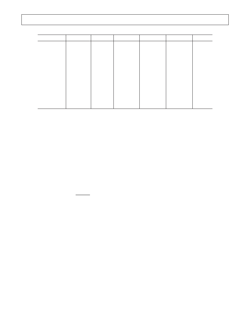
Table III. SSB rCIC2 Alias Rejection Table (f
SAMP
= 1) Bandwidth Shown in Percentage of f
SAMP
M
rCIC2
/L
rCIC2
2
3
4
5
6
7
8
9
10
11
12
13
14
15
16
–50 dB
–60 dB
–70 dB
–80 dB
–90 dB
–100 dB
1.79
1.508
1.217
1.006
0.853
0.739
0.651
0.581
0.525
0.478
0.439
0.406
0.378
0.353
0.331
1.007
0.858
0.696
0.577
0.49
0.425
0.374
0.334
0.302
0.275
0.253
0.234
0.217
0.203
0.19
0.566
0.486
0.395
0.328
0.279
0.242
0.213
0.19
0.172
0.157
0.144
0.133
0.124
0.116
0.109
0.318
0.274
0.223
0.186
0.158
0.137
0.121
0.108
0.097
0.089
0.082
0.075
0.07
0.066
0.061
0.179
0.155
0.126
0.105
0.089
0.077
0.068
0.061
0.055
0.05
0.046
0.043
0.04
0.037
0.035
0.101
0.087
0.071
0.059
0.05
0.044
0.038
0.034
0.031
0.028
0.026
0.024
0.022
0.021
0.02
相關(guān)PDF資料 |
PDF描述 |
|---|---|
| AD6634PCB | 80 MSPS, Dual-Channel WCDMA Receive Signal Processor (RSP) |
| AD6635 | 4-Channel, 80 MSPS WCDMA Receive Signal Processor (RSP) |
| AD6635BB | 4-Channel, 80 MSPS WCDMA Receive Signal Processor (RSP) |
| AD6636 | 150 MSPS Wideband Digital Down-Converter (DDC) |
| AD6636BBCZ1 | 150 MSPS Wideband Digital Down-Converter (DDC) |
相關(guān)代理商/技術(shù)參數(shù) |
參數(shù)描述 |
|---|---|
| AD6634BBCZ | 功能描述:IC RSP 80MSPS DUAL 196CSPBGA RoHS:是 類別:RF/IF 和 RFID >> RF 混頻器 系列:AD6634 產(chǎn)品培訓(xùn)模塊:Lead (SnPb) Finish for COTS Obsolescence Mitigation Program 標(biāo)準(zhǔn)包裝:100 系列:- RF 型:W-CDMA 頻率:2.11GHz ~ 2.17GHz 混頻器數(shù)目:1 增益:17dB 噪音數(shù)據(jù):2.2dB 次要屬性:- 電流 - 電源:11.7mA 電源電壓:2.7 V ~ 3.3 V 包裝:托盤 封裝/外殼:12-VFQFN 裸露焊盤 供應(yīng)商設(shè)備封裝:12-QFN-EP(3x3) |
| AD6634BC/PCB | 制造商:Analog Devices 功能描述:WCDMA RECEIVE SGNL PROCESSOR - Bulk |
| AD6634PCB | 制造商:AD 制造商全稱:Analog Devices 功能描述:80 MSPS, Dual-Channel WCDMA Receive Signal Processor (RSP) |
| AD6635 | 制造商:AD 制造商全稱:Analog Devices 功能描述:4-Channel, 80 MSPS WCDMA Receive Signal Processor (RSP) |
| AD6635BB | 功能描述:IC RSP 80MSPS QUAD 324-BGA RoHS:否 類別:RF/IF 和 RFID >> RF 混頻器 系列:AD6635 產(chǎn)品培訓(xùn)模塊:Lead (SnPb) Finish for COTS Obsolescence Mitigation Program 標(biāo)準(zhǔn)包裝:100 系列:- RF 型:W-CDMA 頻率:2.11GHz ~ 2.17GHz 混頻器數(shù)目:1 增益:17dB 噪音數(shù)據(jù):2.2dB 次要屬性:- 電流 - 電源:11.7mA 電源電壓:2.7 V ~ 3.3 V 包裝:托盤 封裝/外殼:12-VFQFN 裸露焊盤 供應(yīng)商設(shè)備封裝:12-QFN-EP(3x3) |
發(fā)布緊急采購,3分鐘左右您將得到回復(fù)。