- 您現(xiàn)在的位置:買賣IC網(wǎng) > PDF目錄373886 > AD6190ARSRL (ANALOG DEVICES INC) 900 MHz RF Transceiver PDF資料下載
參數(shù)資料
| 型號: | AD6190ARSRL |
| 廠商: | ANALOG DEVICES INC |
| 元件分類: | 無繩電話/電話 |
| 英文描述: | 900 MHz RF Transceiver |
| 中文描述: | TELECOM, CORDLESS, BASEBAND CIRCUIT, PDSO28 |
| 封裝: | SSOP-28 |
| 文件頁數(shù): | 6/8頁 |
| 文件大小: | 150K |
| 代理商: | AD6190ARSRL |
AD6190
–6–
REV. 0
PRODUCT DE SCRIPT ION
T he AD6190 is a complete RF/IF transceiver for operation in
the 902 MHz–928 MHz Industrial, Scientific and Medical
(“ISM”) frequency band. T ogether with a suitable spread-
spectrum controller, the AD6190 can be used to design
a spread-spectrum system compliant with FCC “Part 15”
(47CFR15.247) regulations. T he AD6190 is a fully compatible
companion chip to the Zilog Z87L00 “ZPhone” frequency-
hopping spread-spectrum controller.
T he AD6190 includes a receive path of LNA, image-reject
mixer, IF amplifier and limiter amplifier with RSSI. T he trans-
mit path accepts a 10.7 MHz IF input signal, and uses image-
reject upconversion to the 902 MHz–928 MHz band. Frequency
control is achieved using an on-chip VCO and dual-modulus
prescaler connected to an inexpensive low frequency PLL for
channel selection and frequency hopping.
Additionally, an on-chip voltage regulator stabilizes the VCO to
prevent LO pushing due to power supply variations.
APPLY ING T HE AD6190
Receive Signal Path
T he AD6190 Low Noise Amplifier (LNA) and image-reject
mixer together provide downconverter with a total gain of 24 dB
and a typical Noise Figure (NF) of 4.2 dB.
T he L NA input port exhibits an impedance of 320-j61 at
915 MHz. In order to provide an optimum match to a 50
source, the network shown in Figure 8 should be used.
RF IN
82pF
2.2pF
15nH
50
V
AD6190
Figure 8. LNA Input Matching Circuit
T he frequency plan of the AD6190 provides the lowest possible
RF implementation cost. A single conversion design is used with
a 10.7 MHz IF to take advantage of the very low cost filters
available. However, since the 902 MHz–928 MHz band is wider
than twice the IF, it is possible that undesired in-band signals
will be mixed down to the IF. T hese images could cause inter-
ference to the desired signal. It is thus necessary to provide
tunable filtering before the receive mixer, or some other ap-
proach to eliminate interference from image signals.
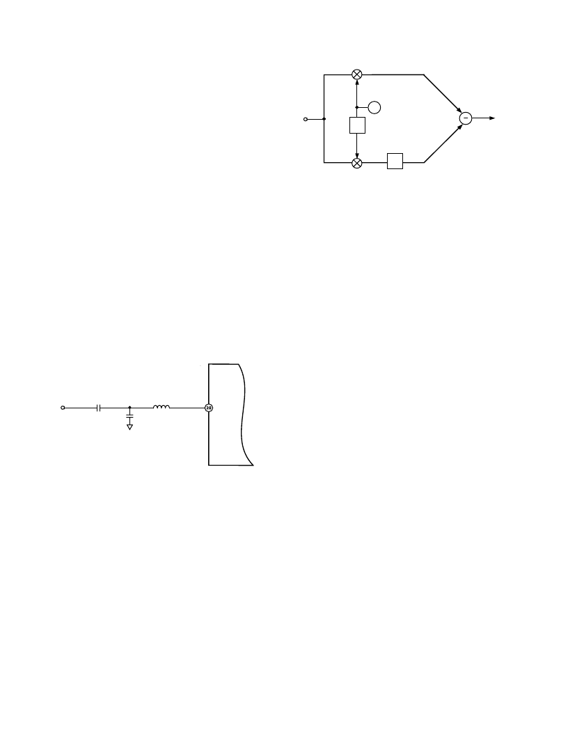
In the AD6190, a technique known as “image-reject” (or SSB)
mixing is used. T his technique suppresses image interference by
using a pair of mixers with quadrature local oscillators. See
Figure 9.
90
8
LO
90
8
IF
OUT
RF
IN
AD6190
Figure 9. Image-Reject Mixer
T he RF signal, containing both the desired signal at (F
LO
+ F
IF
)
and another possible signal at the image frequency of (F
LO
– F
IF
) is
applied to two mixers in parallel. T hese mixers are driven by
local oscillator signals in quadrature. T he mixer outputs at the
two mixer IF ports contain both the desired signal and the
image signal. However, the outputs of the two mixers are in
quadrature (shifted 90 degrees relative to each other). T he
outputs of the two mixers are then shifted another 90 degrees
relative to each other in a phase-shift network. T he two mixer
outputs thus contain the desired signal and the image signal
exactly 180 degrees out of phase. By adding (or subtracting) the
two signals, the undesired image signals cancel, the desired
signal components add, and image-rejection occurs. Local oscil-
lator leakage is suppressed by the use of doubly-balanced mixers.
T he quality of the image rejection is a function of the phase and
amplitude matching of the quadrature branches of the LO and
IF phase-shift networks. In the AD6190, image-rejection is
typically 33 dB.
T he mixer output that drives the input side of the first
10.7 MHz filter should also be connected through a parallel
RLC network of 6.8 pF, 1 k
, and 7 pF to the power supply to
match the 330
filter impedance.
T he 10.7 MHz IF signal is then filtered and amplified by a
24 dB fixed gain. T he output of this stage is further filtered, and
applied to a 6-stage limiting amplifier. T he limiter output signal
is typically 450 mV p-p into a 30 k
, 30 pF load, with a dc
offset level of approximately 1.76 V dc.
All 10.7 MHz IF filters are assumed to be standard 330
imped-
ance ceramic types. T he AD6190 RX IF signal chain and T X IF
input includes internal matching resistors for this impedance.
When used with the Zilog Z87L00 Spread-Spectrum Controller
IC, the 10.7 MHz IF signal contains the received data encoded in
FSK modulation with approximately a
±
33 kHz deviation. T he
Z87L00 performs the FSK demodulation in the digital domain.
T he RSSI (Received Signal Strength Indicator) signal represents
the strength of the received signal, linear in dB, and scales with
supply voltage. With a 3.3 V supply (through a 10
resistor on
the VCCIF pin), an RF signal level of –100 dBm at the LNA
input will produce an RSSI voltage of approximately 900 mV.
T he RSSI voltage will increase with increasing RF input level,
at approximately 22 mV/dB to approximately 2.4 V at
–30 dBm input. T he RSSI output voltage remains above 2.4 V
for input levels up to +15 dBm.
相關PDF資料 |
PDF描述 |
|---|---|
| AD6190ARS | 900 MHz RF Transceiver |
| AD620(中文) | Low Cost, Low Power Instrumentation Amplifier(儀器用放大器) |
| AD620BR-REEL | Precision Instrumentation Amplifier |
| AD620BR-REEL7 | JOYSTICK 4000 POTENTIOMETER |
| AD620AR-REEL | Precision Instrumentation Amplifier |
相關代理商/技術參數(shù) |
參數(shù)描述 |
|---|---|
| AD619BRT | 制造商:Analog Devices 功能描述:- Bulk |
| AD61F08KAC | 制造商:未知廠家 制造商全稱:未知廠家 功能描述:THYRISTOR MODULE|DOUBLER|HALF-CNTLD|POSITIVE|15V V(RRM)|60A I(T) |
| AD61F08KAF | 制造商:未知廠家 制造商全稱:未知廠家 功能描述:THYRISTOR MODULE|DOUBLER|HALF-CNTLD|POSITIVE|15V V(RRM)|60A I(T) |
| AD61F08KBC | 制造商:未知廠家 制造商全稱:未知廠家 功能描述:THYRISTOR MODULE|DOUBLER|HALF-CNTLD|POSITIVE|15V V(RRM)|60A I(T) |
| AD61F08KBF | 制造商:未知廠家 制造商全稱:未知廠家 功能描述:THYRISTOR MODULE|DOUBLER|HALF-CNTLD|POSITIVE|15V V(RRM)|60A I(T) |
發(fā)布緊急采購,3分鐘左右您將得到回復。