- 您現(xiàn)在的位置:買賣IC網(wǎng) > PDF目錄373886 > AD6121ARSRL (ANALOG DEVICES INC) CDMA 3 V Receiver IF Subsystem with Integrated Voltage Regulator PDF資料下載
參數(shù)資料
| 型號: | AD6121ARSRL |
| 廠商: | ANALOG DEVICES INC |
| 元件分類: | 通信及網(wǎng)絡(luò) |
| 英文描述: | CDMA 3 V Receiver IF Subsystem with Integrated Voltage Regulator |
| 中文描述: | SPECIALTY TELECOM CIRCUIT, DSO28 |
| 封裝: | SSOP-28 |
| 文件頁數(shù): | 11/16頁 |
| 文件大小: | 258K |
| 代理商: | AD6121ARSRL |
AD6121
–11–
REV. B
AD6121
IFOPP
IFOPN
2C
PAR
2C
PAR
L/2
L/2
V
CC
10nF
10nF
10nF
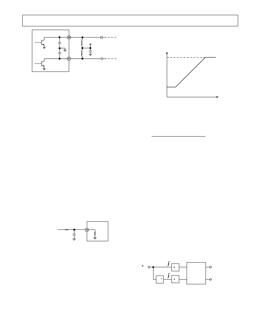
Figure 28. IF Amplifiers’ Output Configuration When
I and Q Demodulator Is Powered Down
In order to confirm whether the pull-up inductors have been
properly designed, sweep the IF frequency and view the output
of the IF amplifiers on a spectrum analyzer. If the inductor
value is correct, the signal should peak at the IF frequency.
The gain of the two amplifier sections (input stage followed by
amplifiers) changes sequentially for optimum signal-to-noise
ratio. For example, in CDMA mode, the gain of the CDMA
input amplifier first increases to maximum and then the gain of
the cascaded IF amplifiers increases to maximum. Likewise, when
decreasing gain, the gain of the cascaded amplifiers decreases to
minimum before the gain of the CDMA input amplifier.
The gain control circuits contain both temperature compensa-
tion circuitry and a choice of internal or external reference for
adjusting the gain scale factor. The gain control input accepts an
external gain control voltage from a DAC. It provides 94.5 dB
of gain control range with a nominal 52.5 dB/V scale factor.
Either an internal or external reference may be used to set the
gain control scale factor.
The external gain control input signal should be free of noise. In
a typical wireless application, it is recommended to filter this
signal in order to reduce the noise that results from the DAC
that generates it. A simple RC filter can be employed, but care
should be taken with its design. If too big a resistor is used, a
large voltage drop may occur across the resistor resulting in
lower gain than expected (as a result of a lower voltage reaching
the AD6121). An RC filter with a 1 kHz bandwidth, employing
a 1 k
resistor is appropriate. This results in a 150 nF capacitor.
The resulting circuit is shown in Figure 29.
AD6121
VGAIN
150nF
1k
FROM
BASEBAND
CONVERTER
100k
Figure 29. Gain Voltage Filtering
The AD6121
’
s overall gain, expressed in decibels, is linear in
dB with respect to the automatic gain control (AGC) voltage,
VGAIN. Either REFOUT, or an external reference voltage
connected to REFIN, may be used to set the voltage range for
VGAIN. When the internal 1.23 V reference, REFOUT, is
connected to REFIN, VGAIN will control the AGC range when
it is typically set between 0.5 V and 2.5 V. Minimum gain oc-
curs at minimum voltage on VGAIN and maximum gain occurs
at maximum voltage on VGAIN. The maximum and minimum
gain will not change with a change in voltage at REFIN. Rather,
the slope of the gain curve will change as a result of a change in
the required range for VGAIN. Figure 30 shows the piecewise
linear approximation of the gain curve for the AD6121.
MAXIMUM
GAIN
MINIMUM
GAIN
VGAIN
–
Volts
G
–
Figure 30. Piecewise Linear Approximation for the
AD6121 Gain Curve
Because the minimum and maximum gains for the AD6121 are
constant, we can approximate the VGAIN range for a given
REFIN voltage by using Equation 2.
Where
MaxGain
is the maximum gain (+47 dB) in dB,
MinGain
is the minimum gain (
–
47.5 dB) in dB,
REFIN
is the reference
input voltage, in volts,
VGAIN
is the gain control voltage input,
in volts, and GAIN is the particular gain, in dB, we would have
for a given REFIN and VGAIN. Consequently, for any REFIN
we choose, we can calculate the VGAIN range by solving Equa-
tion 2 for VGAIN. For example, in order to determine the
VGAIN value for the maximum gain condition, given a 1.23 V
REFIN, we can solve Equation 2 for VGAIN by substituting
47 dB for GAIN and MaxGain,
–
47.5 dB for MinGain and
1.23 V for REFIN. VGAIN can then be calculated to be 2.46
V, or approximately 2.5 V. For the minimum gain condition,
we can determine the VGAIN value by substituting 47 dB for
MaxGain,
–
47.5 dB for Gain and MinGain and 1.23 V for
REFIN. VGAIN can then be calculated to be 0.492 V or ap-
proximately 0.5 V.
I and Q Demodulator
The I and Q demodulator provides differential quadrature base-
band outputs to CDMA baseband converters. The demodulator
provides 5.6 dB of voltage gain in addition to the gain provided
by the IF amplifier stage. The outputs of the I and Q demodula-
tor are filtered with a low-pass filter, which typically has a 16 MHz
bandwidth. A divide-by-two quadrature generator followed by
dual polyphase filters ensures a typical
±
1
°
quadrature accuracy
(Figure 31).
VGAIN
GAIN
(
MinGain
MaxGain MinGain
–
REFIN
REFIN
=
×
+
–
)
.
.
1 6
0 4
(2)
2
180
POLYPHASE
FILTERS
I
Q
I
Q
2 IF
LO INPUT
QUADRATURE
OUTPUT TO
DEMODULATOR
2
Figure 31. Simplified Quadrature Generator Circuit
相關(guān)PDF資料 |
PDF描述 |
|---|---|
| AD6121ACP | CDMA 3 V Receiver IF Subsystem with Integrated Voltage Regulator |
| AD6121ARS | CDMA 3 V Receiver IF Subsystem with Integrated Voltage Regulator |
| AD6121 | CDMA 3 V Receiver IF Subsystem with Integrated Voltage Regulator |
| AD6121ACPRL | CDMA 3 V Receiver IF Subsystem with Integrated Voltage Regulator |
| AD6122ARSRL | CDMA 3 V Transmitter IF Subsystem with Integrated Voltage Regulator |
相關(guān)代理商/技術(shù)參數(shù) |
參數(shù)描述 |
|---|---|
| AD6122 | 制造商:AD 制造商全稱:Analog Devices 功能描述:CDMA 3 V Transmitter IF Subsystem with Integrated Voltage Regulator |
| AD6122ACP | 制造商:Analog Devices 功能描述:COMMUNICATION CDMA 3V TRANSMITTER IF SUBSYSTEM 28SSOP |
| AD6122ACPRL | 制造商:AD 制造商全稱:Analog Devices 功能描述:CDMA 3 V Transmitter IF Subsystem with Integrated Voltage Regulator |
| AD6122ARS | 制造商:AD 制造商全稱:Analog Devices 功能描述:CDMA 3 V Transmitter IF Subsystem with Integrated Voltage Regulator |
| AD6122ARSRL | 制造商:AD 制造商全稱:Analog Devices 功能描述:CDMA 3 V Transmitter IF Subsystem with Integrated Voltage Regulator |
發(fā)布緊急采購,3分鐘左右您將得到回復(fù)。