- 您現(xiàn)在的位置:買賣IC網(wǎng) > PDF目錄373886 > AD605BRZ-RL (ANALOG DEVICES INC) Dual, Low Noise, Single-Supply Variable Gain Amplifier PDF資料下載
參數(shù)資料
| 型號: | AD605BRZ-RL |
| 廠商: | ANALOG DEVICES INC |
| 元件分類: | 模擬信號調(diào)理 |
| 英文描述: | Dual, Low Noise, Single-Supply Variable Gain Amplifier |
| 中文描述: | SPECIALTY ANALOG CIRCUIT, PDSO16 |
| 封裝: | LEAD FREE, MS-012-AC, SOIC-16 |
| 文件頁數(shù): | 13/20頁 |
| 文件大小: | 278K |
| 代理商: | AD605BRZ-RL |
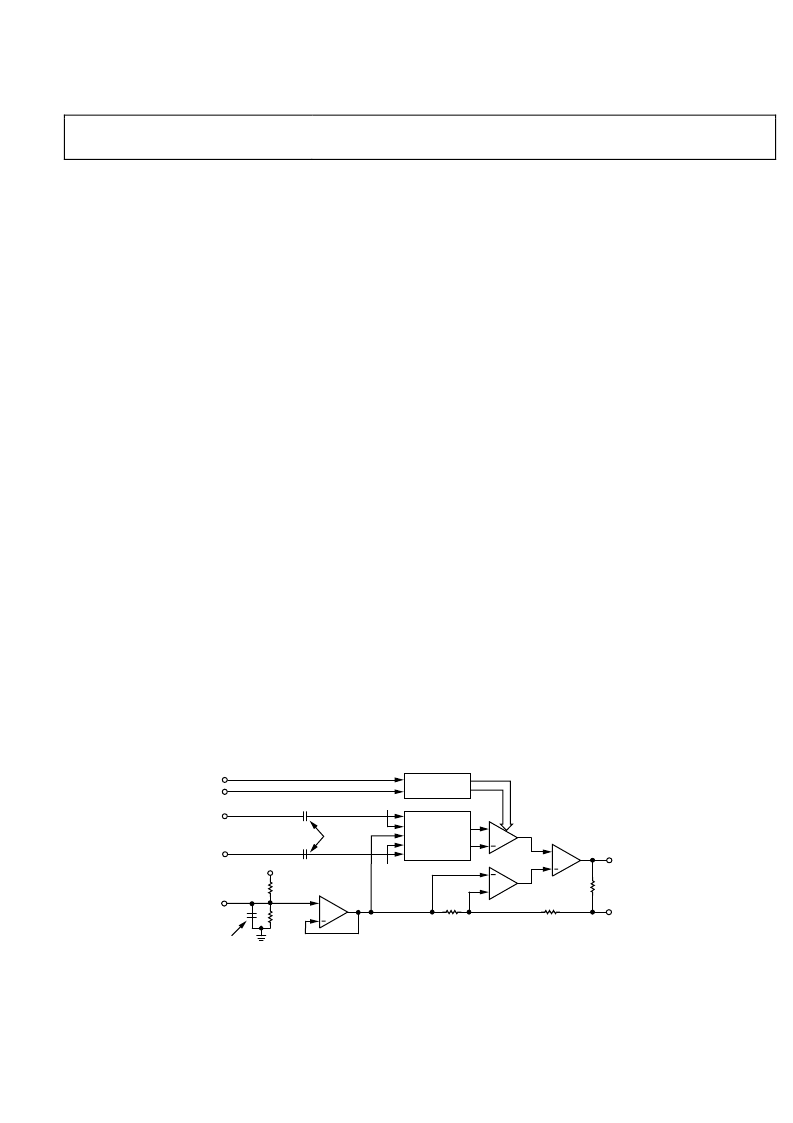
AD605
THEORY OF OPERATION
The AD605 is a dual channel, low noise variable gain amplifier.
Figure 35 shows the simplified block diagram of one channel.
Each channel consists of a single-supply X-AMP (hereafter
called DSX, differential single-supply X-AMP) comprised of:
Rev. D | Page 13 of 20
1
To understand the active-feedback amplifier topology, refer to the
AD830
data sheet. The AD830 is a practical implementation of the idea.
Precision passive attenuator (differential ladder)
Gain control block
VOCM buffer with supply splitting resistors R3 and R4
Active feedback amplifier
1
(AFA) with gain setting
resistors R1 and R2
The linear-in-dB gain response of the AD605 can generally be
described by Equation 1.
G
(dB) = (
Gain Scaling
(dB/V)) × (
Gain Control
(V))
(19 dB (14 dB) × (
FB
))
(1)
where:
FB
= 0, if FBK-to-OUT are shorted.
FB
= 1, if FBK-to-OUT is open.
Each channel provides between 14 dB to +34.4 dB through
0 dB to +48.4 dB of gain depending on the value of the
resistance connected between Pin FBK and Pin OUT. The
center 40 dB of gain is exactly linear-in-dB while the gain error
increases at the top and bottom of the range. The gain is set by
the gain control voltage (VGN). The VREF input establishes the
gain scaling. The useful gain scaling range is between 20 dB/V
and 40 dB/V for a VREF voltage of 2.5 V and 1.25 V,
respectively. For example, if FBK to OUT were shorted and
VREF were set to 2.50 V (to establish a gain scaling of 20 dB/V),
the gain equation would simplify to
G
(dB) = (20 (dB/V)) × (
VGN
(V)) – 19 dB
(2)
The desired gain can then be achieved by setting the unipolar
gain control (VGN) to a voltage within its nominal operating
range of 0.25 V to 2.65 V (for 20 dB/V gain scaling). The gain is
monotonic for a complete gain control range of 0.1 V to 2.9 V.
Maximum gain can be achieved at a VGN of 2.9 V.
Because the two channels are identical, only Channel 1 is used
to describe their operation. VREF and VOCM are the only
inputs that are shared by the two channels, and because they are
normally ac grounds, crosstalk between the two channels is
minimized. For highest gain scaling accuracy, VREF should
have an external low impedance voltage source. For low accuracy
20 dB/V applications, the VREF input can be decoupled with a
capacitor to ground. In this mode, the gain scaling is determined
by the midpoint between +VCC and GND; therefore, care should
be taken to control the supply voltage to 5 V The input resistance
looking into the VREF pin is 10 kΩ ± 20%.
The AD605 is a single-supply circuit and the VOCM pin is used
to establish the dc level of the midpoint of this portion of the
circuit. VOCM needs only an external decoupling capacitor to
ground to center the midpoint between the supply voltages (5 V,
GND). However, if the dc level of the output is important to the
user (see the Applications section of the
AD9050
data sheet for
an example), then VOCM can be specifically set. The input
resistance looking into the VOCM pin is 45 kΩ ± 20%.
R1
820
VREF
VGN
VPOS
VOCM
R3
200k
C3
OUT
DISTRIBUTED G
M
175
175
G1
GAIN
CONTROL
Ao
G2
+
R2
20
R4
200k
EXT
+IN
–IN
FBK
3.36k
DIFFERENTIAL
ATTENUATOR
EXT
C2
C1
0
+
+
+
Figure 35. Simplified Block Diagram of a Single Channel of the AD605
相關PDF資料 |
PDF描述 |
|---|---|
| AD605BRZ-RL7 | Dual, Low Noise, Single-Supply Variable Gain Amplifier |
| AD605 | Dual, Low Noise, Single-Supply Variable Gain Amplifier |
| AD605-EB | Dual, Low Noise, Single-Supply Variable Gain Amplifier |
| AD605ACHIPS | Dual, Low Noise, Single-Supply Variable Gain Amplifier |
| AD605AR-REEL | Dual, Low Noise, Single-Supply Variable Gain Amplifier |
相關代理商/技術參數(shù) |
參數(shù)描述 |
|---|---|
| AD605BRZ-RL7 | 制造商:AD 制造商全稱:Analog Devices 功能描述:Dual, Low Noise, Single-Supply Variable Gain Amplifier |
| AD605-EB | 制造商:Analog Devices 功能描述: |
| AD605EHDK42GMS | 制造商:Advanced Micro Devices 功能描述:EB E64 4C 605E AM3 45W - Trays |
| AD605-EVALZ | 功能描述:BOARD EVALUATION FOR AD605 RoHS:是 類別:編程器,開發(fā)系統(tǒng) >> 評估板 - 運算放大器 系列:X-AMP® 產(chǎn)品培訓模塊:Lead (SnPb) Finish for COTS Obsolescence Mitigation Program 標準包裝:1 系列:- |
| AD606 | 制造商:AD 制造商全稱:Analog Devices 功能描述:50 MHz, 80 dB Demodulating Logarithmic Amplifier with Limiter Output |
發(fā)布緊急采購,3分鐘左右您將得到回復。