- 您現(xiàn)在的位置:買(mǎi)賣(mài)IC網(wǎng) > PDF目錄362093 > AD5539SQ Voltage-Feedback Operational Amplifier PDF資料下載
參數(shù)資料
| 型號(hào): | AD5539SQ |
| 英文描述: | Voltage-Feedback Operational Amplifier |
| 中文描述: | 電壓反饋運(yùn)算放大器 |
| 文件頁(yè)數(shù): | 4/16頁(yè) |
| 文件大小: | 569K |
| 代理商: | AD5539SQ |
第1頁(yè)第2頁(yè)第3頁(yè)當(dāng)前第4頁(yè)第5頁(yè)第6頁(yè)第7頁(yè)第8頁(yè)第9頁(yè)第10頁(yè)第11頁(yè)第12頁(yè)第13頁(yè)第14頁(yè)第15頁(yè)第16頁(yè)
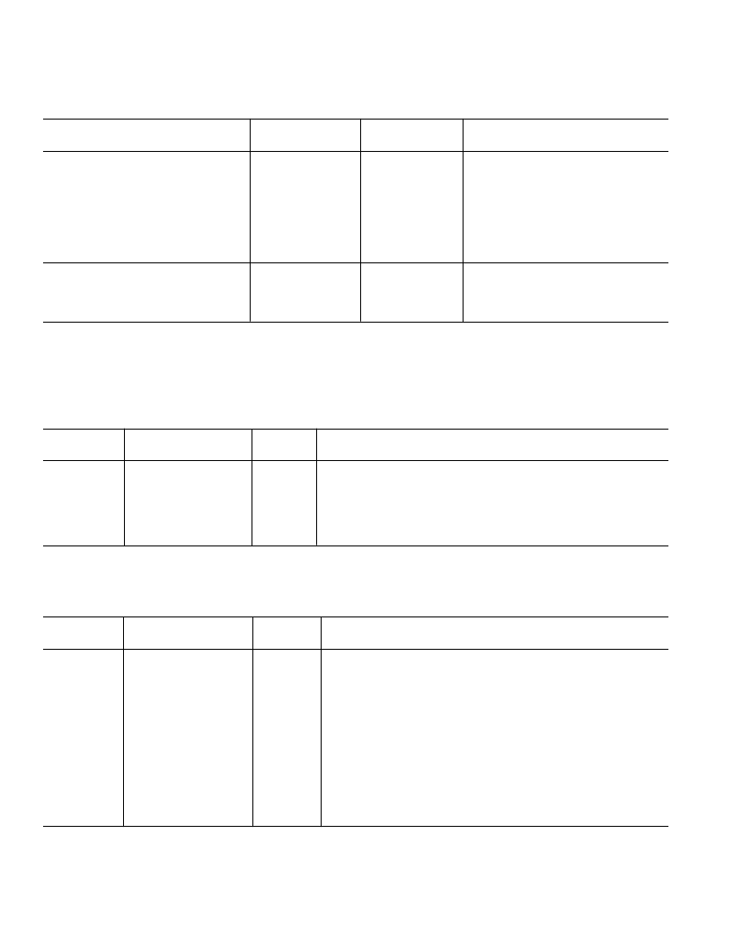
REV. A
–4–
AD5532B-1
B Version
2
Parameter
1
DAC AC CHARACTERISTICS
3
Output Voltage Settling Time
OFFS_IN Settling Time
Digital-to-Analog Glitch Impulse
Digital Crosstalk
Analog Crosstalk
Digital Feedthrough
Output Noise Spectral Density @ 1 kHz
Unit
Conditions/Comments
22
10
1
5
1
0.2
400
μ
s max
μ
s max
nV-s
typ
nV-s
typ
nV-s
typ
nV-s
typ
nV/
√
Hz
typ
500 pF, 5 k
Load Full-Scale Change
500 pF, 5 k
Load; 0 V to 3 V Step
1 LSB Change Around Major Carry
ISHA AC CHARACTERISTICS
Output Voltage Settling Time
3
Acquisition Time
AC Crosstalk
3
3
16
5
μ
s max
μ
s max
nV-s
typ
Outputs Unloaded
NOTES
1
See Terminology section.
2
B Version: Industrial temperature range –40
°
C to +85
°
C; typical at +25
°
C.
3
Guaranteed by design and characterization, not production tested.
Specifications subject to change
without notice.
TIMING CHARACTERISTICS
PARALLEL INTERFACE
Limit at T
MIN
, T
MAX
Parameter
1, 2
(B Version)
Unit
Conditions/Comments
t
1
t
2
t
3
t
4
t
5
t
6
0
0
50
50
20
7
ns min
ns min
ns min
ns min
ns min
ns min
CS
to
WR
Setup Time
CS
to
WR
Hold Time
CS
Pulsewidth Low
WR
Pulsewidth Low
A4–A0, CAL, OFFS_SEL to
WR
Setup Time
A4–A0, CAL, OFFS_SEL to
WR
Hold Time
NOTES
1
See Parallel Interface Timing Diagram.
2
Guaranteed by design and characterization, not production tested.
Specifications subject to change without notice.
SERIAL INTERFACE
Limit at T
MIN
, T
MAX
(B Version)
Parameter
1, 2
f
CLKIN3
t
1
t
2
t
3
t
4
t
5
t
6
t
7
t
84
t
94
t
10
t
t
11
Unit
Conditions/Comments
14
28
28
15
50
15
5
5
20
60
400
400
7
MHz max
ns min
ns min
ns min
ns min
ns min
ns min
ns min
ns max
ns max
ns min
ns min
ns min
SCLK Frequency
SCLK High Pulsewidth
SCLK Low Pulsewidth
SYNC
Falling Edge to SCLK Falling Edge Setup Time
SYNC
Low Time
D
IN
Setup Time
D
IN
Hold Time
SYNC
Falling Edge to SCLK Rising Edge Setup Time for Readback
SCLK Rising Edge to D
OUT
Valid
SCLK Falling Edge to D
OUT
High Impedance
10th SCLK Falling Edge to
SYNC
Falling Edge for Readback
24th SCLK Falling Edge to
SYNC
Falling Edge for DAC Mode Write
SCLK Falling Edge to
SYNC
Falling Edge for Readback
NOTES
1
See Serial Interface Timing Diagrams.
2
Guaranteed by design and characterization, not production tested.
3
In ISHA mode the maximum SCLK frequency is 20 MHz and the minimum pulsewidth is 20 ns.
4
These numbers are measured with the load circuit of Figure 2.
5
SYNC
should be taken low while SCLK is low for readback.
Specifications subject to change without notice.
AD5532B
AC CHARACTERISTICS
(V
DD
= +8 V to +16.5 V, V
SS
= –4.75 V to –16.5 V; AV
CC
= +4.75 V to +5.25 V; DV
CC
= +2.7 V to +5.25 V;
AGND = DGND = DAC_GND = 0 V; REF_IN = 3 V; OFF_IN = OV; All specifications T
MIN
to T
MAX
, unless otherwise noted.)
相關(guān)PDF資料 |
PDF描述 |
|---|---|
| AD5564B | Industrial Control IC |
| AD558* | DACPORT Low Cost. Complete uP-Compatible 8-Bit DAC |
| AD558JCHIPS | 8-Bit Digital-to-Analog Converter |
| AD558JP-REEL | 8-Bit Digital-to-Analog Converter |
| AD558SE | 8-Bit Digital-to-Analog Converter |
相關(guān)代理商/技術(shù)參數(shù) |
參數(shù)描述 |
|---|---|
| AD5539SQ/883B | 制造商:未知廠家 制造商全稱(chēng):未知廠家 功能描述:Operational Amplifier |
| AD5541 | 制造商:AD 制造商全稱(chēng):Analog Devices 功能描述:5 V, Serial-Input Voltage-Output, 16-Bit DACs |
| AD5541_12 | 制造商:AD 制造商全稱(chēng):Analog Devices 功能描述:2.7 V to 5.5 V, Serial-Input, Voltage-Output, 16-Bit DACs |
| AD5541A | 制造商:AD 制造商全稱(chēng):Analog Devices 功能描述:2.7 V to 5.5 V, Serial-Input, Voltage-Output, 16-/12-Bit nanoDACs in LFCSP |
| AD5541AACPZ | 制造商:Analog Devices 功能描述:DAC 16BIT +/-2LSB 0.05PPMC 10LFCSP 制造商:Analog Devices 功能描述:DAC, 16BIT, +/-2LSB, 0.05PPMC, 10LFCSP 制造商:Analog Devices 功能描述:DAC, 16BIT, +/-2LSB, 0.05PPMC, 10LFCSP, Resolution (Bits):16bit, Input Channel T 制造商:Analog Devices 功能描述:DAC, 16BIT, +/-2LSB, 0.05PPMC, 10LFCSP, Resolution (Bits):16bit, Input Channel Type:Serial, Supply Voltage Range:2.7V to 5.5V, Digital IC Case Style:LFCSP, No. of Pins:10, Data Interface:Microwire, QSPI, SPI, Supply Current:125A, , RoHS Compliant: Yes |
發(fā)布緊急采購(gòu),3分鐘左右您將得到回復(fù)。