- 您現(xiàn)在的位置:買賣IC網(wǎng) > PDF目錄362092 > AD548BN OP-AMP|SINGLE|BIPOLAR/JFET|DIP|8PIN|PLASTIC PDF資料下載
參數(shù)資料
| 型號: | AD548BN |
| 英文描述: | OP-AMP|SINGLE|BIPOLAR/JFET|DIP|8PIN|PLASTIC |
| 中文描述: | 運(yùn)放|單|雙極/場效應(yīng)|雙酯| 8引腳|塑料 |
| 文件頁數(shù): | 7/12頁 |
| 文件大小: | 430K |
| 代理商: | AD548BN |
AD548
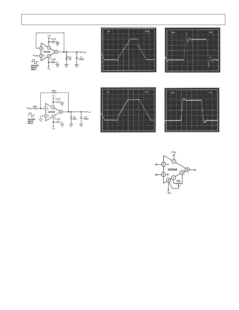
TPC 19c. Unity Gain Follower
Pulse Response (Small Signal)
TPC 19b. Unity Gain Follower
Pulse Response (Large Signal)
TPC 20c. Unity Gain Inverter
Pulse Response (Small Signal)
TPC 20b. Utility Gain Inverter
Pulse Response (Large Signal)
APPLICATION NOTES
The AD548 is a JFET-input op amp with a guaranteed maxi-
mum I
B
of less than 10 pA, and offset and drift laser-trimmed to
0.5 mV and 5
μ
V/
°
C, respectively (AD548B). AC specs include
1 MHz bandwidth, 1.8 V/
μ
s typical slew rate and 8
μ
s settling time
for a 20 V step to
±
0.01%—all at a supply current less than
200
μ
A. To capitalize on the device’s performance, a number of
error sources should be considered.
The minimal power drain and low offset drift of the AD548
reduce self-heating or “warm-up” effects on input offset voltage,
making the AD548 ideal for on/off battery-powered applica-
tions. The power dissipation due to the AD548’s 200
μ
A supply
current has a negligible effect on input current, but heavy out-
put loading will raise the chip temperature. Since a JFET’s
input current doubles for every 10
°
C rise in chip temperature,
this can be a noticeable effect.
The amplifier is designed to be functional with power supply
voltages as low as
±
4.5 V. It will exhibit a higher input offset
voltage than at the rated supply voltage of
±
15 V, due to power
supply rejection effects. The common-mode range of the AD548
extends from 3 V more positive than the negative supply to 1 V
more negative than the positive supply. Designed to cleanly
drive up to 10 k
and 100 pF loads, the AD548 will drive a 2
k
load with reduced open-loop gain.
OFFSET NULLING
Unlike bipolar input amplifiers, zeroing the input offset voltage
of a BiFET op amp will not minimize offset drift. Using balance
Pins 1 and 5 to adjust the input offset voltage as shown in
Figure 1 will induce an added drift of 0.24
μ
V/
°
C per 100
μ
V of
nulled offset. The low initial offset (0.5 mV) of the AD548B
results in only 0.6
μ
V/
°
C of additional drift.
REV. C
–7–
TPC 19a. Unity Gain Follower
TPC 20a. Utility Gain Inverter
Figure 1. Offset Null Configuration
LAYOUT
To take full advantage of the AD548’s 10 pA max input current,
parasitic leakages must be kept below an acceptable level. The
practical limit of the resistance of epoxy or phenolic circuit
board material is between 1
×
10
12
and 3
×
10
12
. This can
result in an additional leakage of 5 pA between an input of 0 V
and a –15 V supply line. Teflon
or a similar low leakage mate-
rial (with a resistance exceeding 10
17
) should be used to
isolate high impedance input lines from adjacent lines carrying
high voltages. The insulator should be kept clean, since con-
taminants will degrade the surface resistance.
A metal guard completely surrounding the high impedance nodes
and driven by a voltage near the common-mode input potential
can also be used to reduce some parasitic leakages. The guarding
pattern in Figure 2 will reduce parasitic leakage due to finite
board surface resistance; but it will not compensate for a low
volume resistivity board.
Teflon is a registered trademark of DuPont.
相關(guān)PDF資料 |
PDF描述 |
|---|---|
| AD548SN | OP-AMP|SINGLE|BIPOLAR/JFET|DIP|8PIN|PLASTIC |
| AD548JN | Precision, Low Power BiFET Op Amp |
| AD548JR | Precision, Low Power BiFET Op Amp |
| AD548JR-REEL | Precision, Low Power BiFET Op Amp |
| AD548KR-REEL | Precision, Low Power BiFET Op Amp |
相關(guān)代理商/技術(shù)參數(shù) |
參數(shù)描述 |
|---|---|
| AD548BQ | 制造商:Rochester Electronics LLC 功能描述:- Bulk |
| AD548BR | 制造商:AD 制造商全稱:Analog Devices 功能描述:Precision, Low Power BiFET Op Amp |
| AD548BR-REEL | 制造商:AD 制造商全稱:Analog Devices 功能描述:Precision, Low Power BiFET Op Amp |
| AD548C | 制造商:AD 制造商全稱:Analog Devices 功能描述:Precision, Low Power BiFET Op Amp |
| AD548CH | 制造商:Analog Devices 功能描述: |
發(fā)布緊急采購,3分鐘左右您將得到回復(fù)。