- 您現(xiàn)在的位置:買(mǎi)賣(mài)IC網(wǎng) > PDF目錄373864 > AD22001 (Analog Devices, Inc.) Circular Connector; MIL SPEC:MIL-DTL-38999 Series I; Body Material:Metal; Series:LJT; No. of Contacts:4; Connector Shell Size:21; Connecting Termination:Crimp; Circular Shell Style:Wall Mount Receptacle; Body Style:Straight RoHS Compliant: No PDF資料下載
參數(shù)資料
| 型號(hào): | AD22001 |
| 廠(chǎng)商: | Analog Devices, Inc. |
| 元件分類(lèi): | 圓形連接器 |
| 英文描述: | Circular Connector; MIL SPEC:MIL-DTL-38999 Series I; Body Material:Metal; Series:LJT; No. of Contacts:4; Connector Shell Size:21; Connecting Termination:Crimp; Circular Shell Style:Wall Mount Receptacle; Body Style:Straight RoHS Compliant: No |
| 中文描述: | 5通道單片比較監(jiān)測(cè)燈 |
| 文件頁(yè)數(shù): | 2/8頁(yè) |
| 文件大?。?/td> | 146K |
| 代理商: | AD22001 |
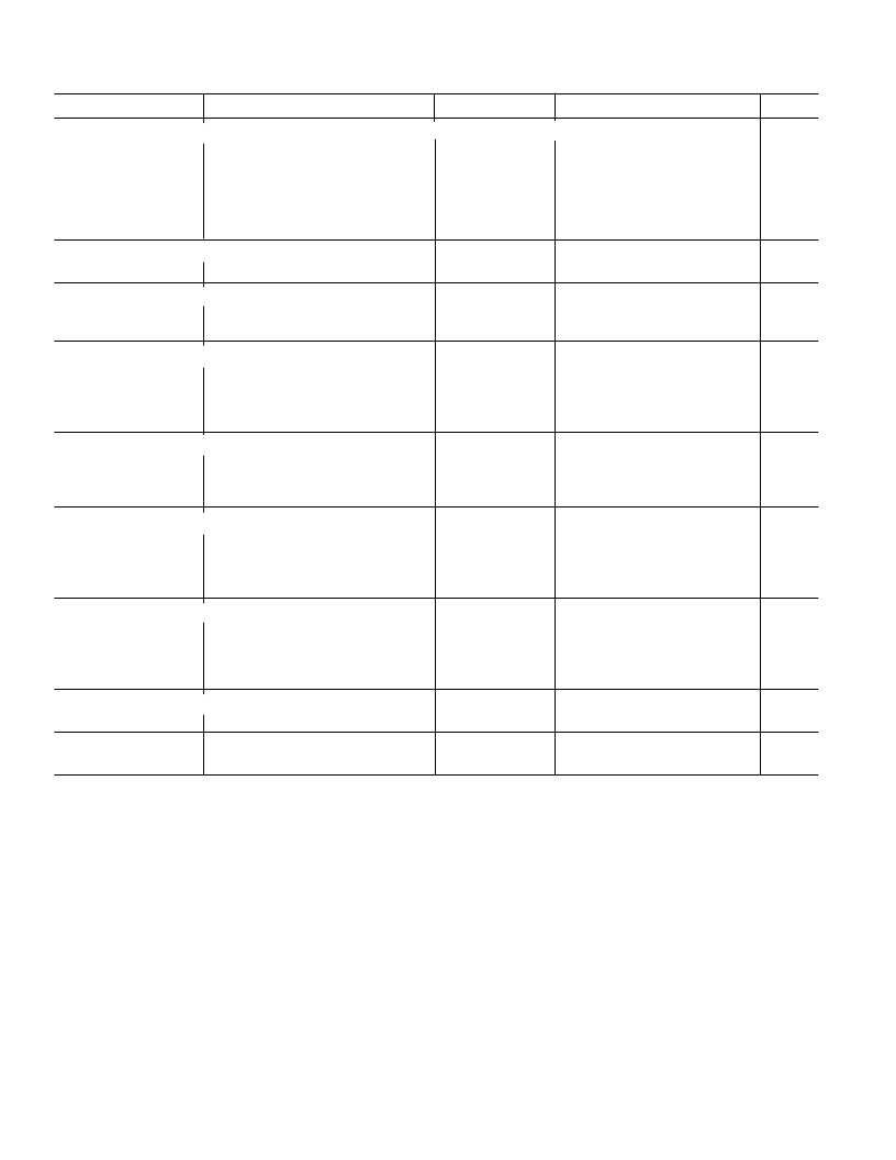
Parameter
T est Conditions
Min
T yp
Max
Units
DIFFERENT IAL INPUT S (Voltage Drop from Shunt Resistor: Pins 4 & 5, 8 & 9, 10 & 11, 14 & 15, 16 & 17)
V
INDIFF
Comparator T hreshold Voltage
1
V
INCM
Common-Mode T hreshold Voltage
1
Power Supply Sensitivity of V
INDIFF2
T emperature Compensation of V
INDIFF3
I
INB
Input Bias Current
I
INC
Constant Current Source
4
1.5
5
1.75
2.0
mV
V
%
ppm/
°
C
μ
A
μ
A
9 V
≤
V
S
≤
16 V
50
3770
10
60
30
SINGLE-ENDED INPUT S (Fuse Monitoring: Pins 6, 19)
V
INF
Fuse Input T hreshold Voltage
5
4
V
CHIP ENABLE CONT ROL INPUT (Pin 1)
V
INCE
V
INCD
Chip Enable, Input High
Chip Disable (Stop Operation)
6
9
V
V
6
OUT PUT S (Pins 7, 12, 13, 18)
V
OUT L
Output Voltage, Low
Indicates No Fault in Lamp Circuit
Output Voltage, High
Indicates Fault in Lamp Circuit
Load = 500
μ
A
0.6
V
V
OUT H
9 V
≤
V
S
≤
V
SSDH
Load = 50
μ
A
V
OUT PS
–2.5
V
OUT PS
V
POWER SUPPLY (Pin 2: +V
S
, Pin 20: GND)
V
S
I
S
Supply Voltage
Quiescent Supply Current
V
OUT H
: No Load
9
1
30
5
V
mA
μ
A
Pin 1 High
Pin 1 Low
3
100
POWER SUPPLY OUT PUT (Pin 3)
V
OUT PS
Power Supply Output Voltage
10 V < V
S
< 14.5 V
V
S
–0.5
I
OUT PS
≤
1 mA
V
S
–0.3
V
S
V
Max Output Voltage
Power Supply Output Current
7
16
18
V
mA
I
OUT PS
2
OPERAT ING SHUT DOWN (Safety Features)
V
SSDH
Operation Shutdown at High
Power Supply Voltages
8
Operation Shutdown at Low
Power Supply Voltage
9
30
33
36
V
V
SSDL
7
9
V
T EMPERAT URE RANGE
T
A
Operating T emperature Range
–40
+125
°
C
PACK AGE
Plastic DIP (N-20)
AD22001N
NOT ES
1
In the presence of a common-mode voltage greater than 5 V, if the shunt voltage applied to the comparator does not exceed the threshold (i.e., the bulb is switched
on but does not draw current), then the device will indicate a failure.
2
At V
= 13.5 V, the differential input threshold voltage is typically 1.75 mV. With an increase of V
, the threshold voltage, V
INDIFF
, will change as well.
Power supply sensitivity of 50% means that when the power supply voltage V
S
increases by 10%, the threshold voltage V
INDIFF
centage value: 5%.
3
T his is the temperature coefficient to compensate for any temperature influence on the external copper PCB track shunt resistors. 3770 ppm/
°
C is equal to 6.6
μ
V/
°
C.
4
T his current source is used to test the lamp when it is switched off (cold lamp test).
5
If the voltage at the input from the fuse (Pin 6 or 19) does not exceed the threshold voltage, then the output will indicate a failure.
6
When the Chip Enable is open-circuited, the chip is disabled.
7
Shorting V
to ground will cause the device to stop operating for that period. However, the device will not suffer any damage.
8
At this voltage, or above, the internal power supply and the power output V
will be shut off.
9
Below the minimum voltage, the circuit will shut down. Above the maximum, the circuit will be on if enabled.
All min and max specifications are guaranteed, although only those marked in
boldface
are tested on all production units at final test.
Specifications subject to change without notice.
REV. A
–2–
AD22001–SPECIFICATIONS
(T
A
= +22
8
C, V
S
= +13.5 V unless otherwse noted)
相關(guān)PDF資料 |
PDF描述 |
|---|---|
| AD22001N | Circular Connector; No. of Contacts:14; Series:LJTPQ00R; Body Material:Aluminum; Connecting Termination:Crimp; Connector Shell Size:23; Circular Contact Gender:Pin; Circular Shell Style:Wall Mount Receptacle |
| AD22001* | 5-Channel Monolithic Comparator for Lamp Monitoring |
| AD22050 | Single-Supply Sensor Interface Amplifier |
| AD22050R-REEL | Single-Supply Sensor Interface Amplifier |
| AD22050N | Single-Supply Sensor Interface Amplifier |
相關(guān)代理商/技術(shù)參數(shù) |
參數(shù)描述 |
|---|---|
| AD22001-2 | 制造商:Analog Devices 功能描述: |
| AD22001N | 制造商:Analog Devices 功能描述: |
| AD22001P | 制造商:Analog Devices 功能描述: |
| AD22002 | 制造商:未知廠(chǎng)家 制造商全稱(chēng):未知廠(chǎng)家 功能描述:Analog IC |
發(fā)布緊急采購(gòu),3分鐘左右您將得到回復(fù)。