- 您現(xiàn)在的位置:買賣IC網(wǎng) > PDF目錄373857 > AD15700BCA (ANALOG DEVICES INC) 1 MSPS 16-/14-Bit Analog I/O Port PDF資料下載
參數(shù)資料
| 型號(hào): | AD15700BCA |
| 廠商: | ANALOG DEVICES INC |
| 元件分類: | 模擬信號(hào)調(diào)理 |
| 英文描述: | 1 MSPS 16-/14-Bit Analog I/O Port |
| 中文描述: | SPECIALTY ANALOG CIRCUIT, PBGA144 |
| 封裝: | MO-205AC, CSPBGA-144 |
| 文件頁數(shù): | 29/44頁 |
| 文件大?。?/td> | 1100K |
| 代理商: | AD15700BCA |
第1頁第2頁第3頁第4頁第5頁第6頁第7頁第8頁第9頁第10頁第11頁第12頁第13頁第14頁第15頁第16頁第17頁第18頁第19頁第20頁第21頁第22頁第23頁第24頁第25頁第26頁第27頁第28頁當(dāng)前第29頁第30頁第31頁第32頁第33頁第34頁第35頁第36頁第37頁第38頁第39頁第40頁第41頁第42頁第43頁第44頁
REV. A
AD15700
–29–
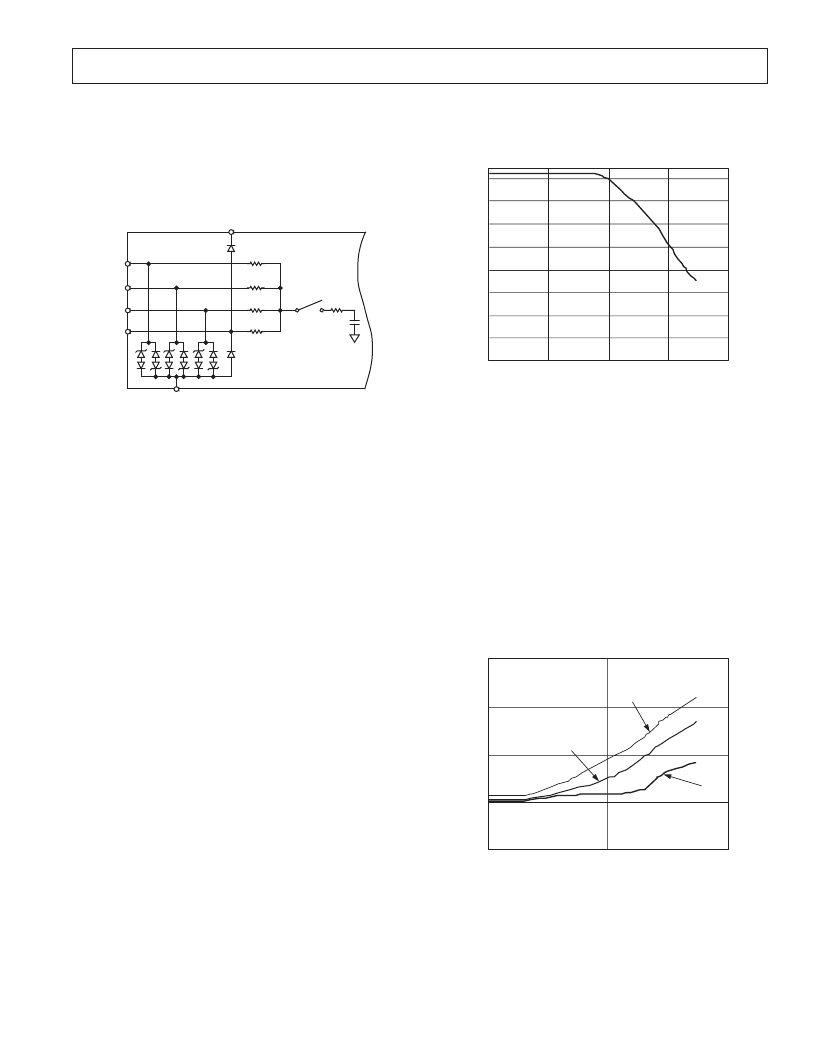
Analog Inputs
The ADC is specified to operate with six full-scale analog input
ranges. Connections required for each of the four analog inputs,
IND, INC, INB, INA, and the resulting full-scale ranges are
shown in Table I. The typical input impedance for each analog
input range is also shown.
Figure 9 shows a simplified analog input section of the ADC.
IND
INC
INB
INA
AVDD
AGND
R = 1.28k
C
S
R1
4R
4
2R
R
Figure 9. Simplified Analog Input
The four resistors connected to the four analog inputs form a
resistive scaler that scales down and shifts the analog input range
to a common input range of 0 V to 2.5 V at the input of the
switched capacitive ADC.
By connecting the four inputs INA, INB, INC, and IND to the
input signal itself, the ground, or a 2.5 V reference, other analog
input ranges can be obtained.
The diodes shown in Figure 9 provide ESD protection for the
four analog inputs. The inputs INB, INC, and IND, have a high
voltage protection (–11 V to +30 V) to allow wide input voltage
range. Care must be taken to ensure that the analog input signal
never exceeds the absolute ratings on these inputs including
INA (0 V to 5 V). This will cause these diodes to become for-
ward-biased and start conducting current. These diodes can
handle a forward-biased current of 120 mA maximum. For
instance, when using the 0 V to 2.5 V input range, these condi-
tions could eventually occur on the input INA when the input
buffer’s (U1) supplies are different from AVDD. In such case,
an input buffer with a short circuit current limitation can be
used to protect the part.
This analog input structure allows the sampling of the differential
signal between the output of the resistive scaler and INGND.
Unlike other converters, the INGND input is sampled at the same
time as the inputs. By using this differential input, small signals
common to both inputs are rejected as shown in Figure 10, which
represents the typical CMRR over frequency. For instance, by
using INGND to sense a remote signal ground, differences of
ground potentials between the sensor and the local ADC ground
are eliminated. During the acquisition phase for ac signals, the
ADC behaves like a one-pole RC filter consisting of the equivalent
resistance of the resistive scaler R/2 in series with R1 and C
S
. The
resistor R1 is typically 100
W
and is a lumped component made
up of some serial resistor and the on resistance of the switches.
The capacitor C
S
is typically 60 pF and is mainly the ADC
sampling capacitor. This one-pole filter with a typical –3 dB
cutoff frequency of 9.6 MHz reduces undesirable aliasing effects
and limits the noise coming from the inputs.
FREQUENCY – kHz
70
C
65
60
55
75
100
50
45
40
35
10
1
1000
10000
Figure 10. Analog Input CMRR vs. Frequency
Except when using the 0 V to 2.5 V analog input voltage range,
the ADC has to be driven by a very low impedance source to
avoid gain errors. That can be done by using the driver amplifier.
When using the 0 V to 2.5 V analog input voltage range, the
input impedance of the ADC is very high so the ADC can be
driven directly by a low impedance source without gain error.
That allows putting an external one-pole RC filter between the
output of the amplifier output and the ADC analog inputs to
even further improve the noise filtering done by the ADC analog
input circuit. However, the source impedance has to be kept low
because it affects the ac performances, especially the total harmonic
distortion (THD). The maximum source impedance depends on
the amount of total THD that can be tolerated. The THD degra-
dation is a function of the source impedance and the maximum
input frequency, as shown in Figure 11.
FREQUENCY – kHz
T
–80
–90
–70
100
–100
–110
0
1000
R = 50
R = 100
R = 11
Figure 11. THD vs. Analog Input Frequency and
Input Resistance (0 V to 2.5 V Only)
相關(guān)PDF資料 |
PDF描述 |
|---|---|
| AD1580A | ECONOLINE: RD & RC - Dual Output from a Single Input Rail- 1kVDC & 2kVDC Isolation- Power Sharing on Output- Custom Solutions Available- UL94V-0 Package Material- Efficiency to 86% |
| AD1580ART | 1.2 V Micropower, Precision Shunt Voltage Reference |
| AD1580ART-REEL1 | 1.2 V Micropower, Precision Shunt Voltage Reference |
| AD1580ART-REEL7 | 1.2 V Micropower, Precision Shunt Voltage Reference |
| AD1580B | ECONOLINE: RD & RC - Dual Output from a Single Input Rail- 1kVDC & 2kVDC Isolation- Power Sharing on Output- Custom Solutions Available- UL94V-0 Package Material- Efficiency to 86% |
相關(guān)代理商/技術(shù)參數(shù) |
參數(shù)描述 |
|---|---|
| AD-1571-1-POWERTACT-HO | 制造商:TE Connectivity 功能描述:AD-1571-1-POWERTACT-HOLDR |
| AD-1571-1-POWERTACT-HOLDR | 功能描述:POWERTACT HOLDR 制造商:te connectivity raychem cable protection 系列:- 零件狀態(tài):在售 配件類型:支座 配套使用產(chǎn)品/相關(guān)產(chǎn)品:同軸連接器 標(biāo)準(zhǔn)包裝:1 |
| AD-1572-1-SOLD-HOLDER- | 制造商:TE Connectivity 功能描述:AD-1572-1-SOLD-HOLDER-ASY |
| AD-1572-1-SOLD-HOLDER-ASY | 功能描述:AD-1572-1-SOLD-HOLDER-ASY 制造商:te connectivity raychem cable protection 系列:* 零件狀態(tài):有效 標(biāo)準(zhǔn)包裝:1 |
| AD-1574-1 | 功能描述:AD-1574-1 制造商:te connectivity raychem cable protection 系列:* 零件狀態(tài):有效 標(biāo)準(zhǔn)包裝:1 |
發(fā)布緊急采購(gòu),3分鐘左右您將得到回復(fù)。